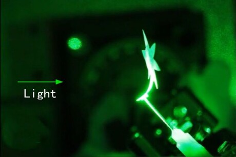
Smart materials move when activated by light

A team of US and Italian researchers, led by Tufts University, has created light-activated composite devices able to execute precise, visible movements and form complex three-dimensional shapes without the need for wires or other actuating materials or energy sources.
Described in the journal Nature Communications, the team’s design combines programmable photonic crystals with an elastomeric composite that can be engineered at the macro and nano scale to respond to illumination.
Colour results from the absorption and reflection of light. Behind every flash of an iridescent butterfly wing or opal gemstone lie complex interactions in which natural photonic crystals embedded in the wing or stone absorb light of specific frequencies and reflect others. The angle at which the light meets the crystalline surface can affect which wavelengths are absorbed and the heat that is generated from that absorbed energy.
The photonic material designed by the Tufts team joins two layers: an opal-like film made of silk fibroin doped with gold nanoparticles (AuNPs), forming photonic crystals, and an underlying substrate of polydimethylsiloxane (PDMS), a silicon-based polymer. In addition to remarkable flexibility, durability and optical properties, silk fibroin is unusual in having a negative coefficient of thermal expansion (CTE), meaning that it contracts when heated and expands when cooled. PDMS, in contrast, has a high CTE and expands rapidly when heated. As a result, when the novel material is exposed to light, one layer heats up much more rapidly than the other, so the material bends as one side expands and the other contracts or expands more slowly.
“With our approach, we can pattern these opal-like films at multiple scales to design the way they absorb and reflect light,” said Professor Fiorenzo Omenetto, corresponding author on the study. “When the light moves and the quantity of energy that’s absorbed changes, the material folds and moves differently as a function of its relative position to that light.”
Whereas most optomechanical devices that convert light to movement involve complex and energy-intensive fabrication or set-ups, “We are able to achieve exquisite control of light-energy conversion and generate ‘macro motion’ of these materials without the need for any electricity or wires,” Prof Omenetto said.
The researchers programmed the photonic crystal films by applying stencils and then exposing them to water vapour to generate specific patterns. The pattern of surface water altered the wavelength of absorbed and reflected light from the film, thus causing the material to bend, fold and twist in different ways, depending on the geometry of the pattern, when exposed to laser light.
The authors demonstrated in their study a ‘photonic sunflower’, with integrated solar cells in the bilayer film so that the cells tracked the light source, with the flower’s petals curling towards and away from illumination. The photonic sunflower kept the angle between the solar cells and the laser beam nearly constant, maximising the cells’ efficiency as the light moved. The team’s demonstrations of the material also included a butterfly whose wings opened and closed in response to light and a self-folding box.
The system would work as well with white light as it does with laser light. Such wireless, light-responsive, heliotropic (sun-following) systems could potentially enhance light-to-energy conversion efficiency for the solar power industry. The research thus provides new avenues for the development of smart light-driven systems, such as high-efficiency, self-aligning solar cells that automatically follow the sun’s direction and angle of light; light-actuated microfluidic valves; and soft robots that move with light on demand.
Please follow us and share on Twitter and Facebook. You can also subscribe for FREE to our weekly newsletter and bimonthly magazine.
Hidden semiconductor activity spotted by researchers
Researchers have discovered that the material that a semiconductor chip device is built on,...
3D reflectors help boost data rate in wireless communications
Cornell researchers have developed a semiconductor chip that will enable smaller devices to...
Scientists revolutionise wireless communication with 3D processors
Scientists have developed a method for using semiconductor technology to manufacture processors...


