Hafnia: unravelling the secrets of next-gen semiconductors

A team of scientists with the U.S. Department of Energy’s Oak Ridge National Laboratory has investigated the behaviour of hafnium oxide, or hafnia, because of its potential for use in novel semiconductor applications. Hafnia exhibits ferroelectricity, which means it is capable of extended data storage even when power is disconnected and therefore can be used in the development of new, so-called non-volatile memory technologies. Innovative non-volatile memory applications could pave the way for the creation of bigger and faster computer systems by alleviating the heat generated from the continual transfer of data to short-term memory.
The scientists researched whether the atmosphere plays a role in hafnia’s ability to change its internal electric charge arrangement when an external electric field is applied. The goal was to explain the range of unusual phenomena that have been obtained in hafnia research. The research findings were published in Nature Materials.
Kyle Kelley, a researcher with the Center for Nanophase Materials Sciences, said the study proved that the ferroelectric behaviour in these systems is coupled to the surface and is tuneable by changing the surrounding atmosphere. Kelley performed the experiments and envisioned the project in collaboration with Sergei Kalinin of the University of Tennessee, Knoxville.
Materials commonly used for memory applications have a surface, or dead, layer that interferes with the material’s ability to store information. As materials are scaled down, the effect of the dead layer becomes extreme enough to stop the functional properties. By changing the atmosphere, the scientists were able to tune the surface layer’s behaviour, which, in hafnia, transitioned the material from the antiferroelectric to the ferroelectric state.
“Ultimately, these findings provide a pathway for predictive modelling and device engineering of hafnia, which is urgently needed, given the importance of this material in the semiconductor industry,” Kelley said.
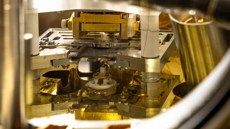
Predictive modelling enables scientists to use previous research to estimate the properties and behaviour of an unknown system. The study that Kelley and Kalinin led focused on hafnia alloyed, or blended, with zirconia, a ceramic material. But future research could apply the findings to anticipate how hafnia may behave when alloyed with other elements. The researchers used atomic force microscopy inside a glovebox and in ambient conditions, as well as ultra-high atomic force microscopy.
“We basically changed the environment all the way from ambient atmosphere to ultrahigh vacuum. In other words, we removed all gases in the atmosphere to negligible levels and measured these responses, which is extremely hard to do,” Kelley said.
Researchers from Carnegie Mellon University provided electron microscopy characterisation, and collaborators from the University of Virginia led the materials development and optimisation. The researchers hope that what they have discovered will stimulate new research specific to exploring the role of controlled surface and interface electrochemistries — the relationship between electricity and chemical reactions — in a computing device’s performance.
“Future studies can extend this knowledge to other systems to help us understand how the interface affects the device properties, which, hopefully, will be in a good way. Typically, the interface kills your ferroelectric properties when scaled to these thicknesses. In this case, it showed us a transition from one material state to another,” Kelley said.
Fully coupled annealing processor for enhanced problem solving
Researchers have designed a scalable, fully-coupled annealing processor with 4096 spins, and...
STMicroelectronics breaks 20 nm barrier for next-gen microcontrollers
STMicroelectronics has launched an advanced process based on 18 nm Fully Depleted Silicon On...
Chip opens door to AI computing at light speed
A team of engineers have developed a silicon-photonics chip that uses light waves, rather than...


