Innovative new method controls optical circuits on PICs

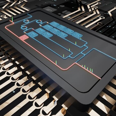
Researchers from Monash University, RMIT and the University of Adelaide have developed a method to control optical circuits on fingernail-sized photonic integrated circuits. The development, published in Optica, builds on the work by the same team who recently created a self-calibrated photonic chip.
Photonics, or the use of light particles to store and transmit information, is a burgeoning field, supporting the need to create faster, better, more efficient and more sustainable technology. Programmable photonic integrated circuits (PICs) offer diverse signal processing functions within a single chip, and present solutions for applications ranging from optical communications to artificial intelligence. Photonics is also changing the processing capability of large-scale equipment onto a chip the size of a human fingernail.
Earlier this year, researchers at Monash University, RMIT and the University of Adelaide developed an advanced photonic circuit that could transform the speed and scale of photonics technology. However, as the scale and complexity of PICs grows, the characterisation and calibration of them becomes increasingly challenging. Monash University research fellow Professor Mike Xu said the team added a common reference path to the chip, which enables stable and accurate measurements of the lengths (phases, time delays) and losses of the ‘workhorse’ paths. “By inventing a new method, the fractional delay method, we have been able to separate out the wanted information from the unwanted, making for more precise applications,” Xu said.
Previously chips have been measured/calibrated by connecting to complex and expensive external equipment (called a vector network analyser); however, the connections to it introduce phase errors, caused by vibrations and temperature changes. By putting the reference on the actual chip, these phase errors can be avoided. Professor Arthur Lowery from Monash University said that previously, researchers used the ‘Kramers–Kronig’ method to remove unwanted errors from desired measurements, but the fractional method requires less optical power for calibration for a given accuracy. “This means that we can get reliable measurements of the chip’s status, so are able to accurately program it for a desired application, such as pattern recognition in an optical computer, or squeezing extra capacity from an optical communications network,” Lowery said.
This work complements research from 2020 that developed a new optical microcomb chip that was able to transfer 30 terabits per second. In the next phase of development, within the ARC Centre of Excellence for Optical Microcombs and Breakthrough Science (COMBS), this research team will explore how photonic chips can use many wavelengths to achieve ultrafast information processing and machine intelligence.
“The complexity of photonic integrated circuits is rapidly increasing, requiring a breakthrough to be able to calibrate and control them. The technique we developed overcomes this challenge, ensuring that the circuits can robustly be used for applications such as pattern recognition,” said Dr Andy Boes from the University of Adelaide.
Fully coupled annealing processor for enhanced problem solving
Researchers have designed a scalable, fully-coupled annealing processor with 4096 spins, and...
STMicroelectronics breaks 20 nm barrier for next-gen microcontrollers
STMicroelectronics has launched an advanced process based on 18 nm Fully Depleted Silicon On...
Chip opens door to AI computing at light speed
A team of engineers have developed a silicon-photonics chip that uses light waves, rather than...


