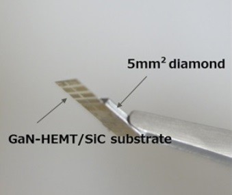
Single-crystal diamond bonded to SiC at room temperature

Fujitsu and Fujitsu Laboratories have announced what is claimed to be the world’s first technology for bonding single-crystal diamond to a silicon carbide (SiC) substrate at room temperature. Using this technology for heat dissipation in a high-power gallium nitride (GaN) high-electron-mobility transistor (HEMT) enables stable operations at high power levels.
In recent years, high-frequency GaN-HEMT power amps have widely been used for long-range radio applications, such as radar and wireless communications. They are also expected to be used in weather radar that observes localised heavy rains, for example, or in the forthcoming 5G millimetre-band mobile communications protocols.
For these types of radars or wireless communications using the microwave to millimetre-wave bands, by raising the output of the GaN-HEMT power amps used for transmissions, the distance that radio waves can propagate will allow the expansion of the observational range of radar while enabling longer and higher capacity communications. This is why GaN-HEMT power amps with higher power output are desirable.
In GaN-HEMT power amps, some of the input power is converted to heat. This heat is dispersed into the SiC substrate, and is carried away by a cooling structure (heat sink). Although the SiC substrate has relatively high thermal conductivity, a material with even better thermal conductivity will be needed for devices with increasingly higher power output to efficiently carry device heat to the cooling structure.
Single-crystal diamond has extremely good thermal conductivity — almost five times that of a SiC substrate — and can efficiently spread heat. In order to bond a single-crystal diamond to a device as a cooling material, normal production processes use an argon (Ar) beam to remove impurities, which produces a low-density damaged surface that weakens the bonds the single-crystal diamond can form. Moreover, using SiN or other insulating films for bonding interferes with thermal conductivity due to SiN’s thermal resistance.
Now, Fujitsu and Fujitsu Laboratories have developed technology for room-temperature bonding of a SiC substrate single-crystal diamond, used for high-efficiency cooling of GaN-HEMT power amps. These two hard materials have different coefficients of thermal expansion.
To prevent the Ar beam from forming a damaged layer on the diamond surface, the companies developed a technique that protects the surface with an extremely thin metallic film before it is exposed to the Ar beam. In order to ensure the surface is planar, for good bonding at room temperature, the metallic film is held to a thickness of 10 nm or less. This prevents the formation of the damaged layer on the diamond surface after Ar beam exposure, resulting in improved bonding strength.
The SiC/diamond interface was found to have an extremely low thermal resistance of 6.7 x 10⁻⁸ m2 K/W. Simulations using this measured parameter showed that the technology would significantly reduce thermal resistance of 200 W-class devices, to 61%. Use of this technology thus promises GaN-HEMT power amps for transmitters with even higher power output.
Fujitsu and Fujitsu Laboratories aim to implement their technology in high-output, high-frequency GaN-HEMT power amps in fiscal 2020, with potential applications expected to include weather radars and 5G wireless communications systems. The power amps could be expected to increase a weather radar’s observable range by a factor of 1.5, allowing for quicker detection of the cumulonimbus clouds and contributing to a safer and more secure society in terms of disaster readiness.
Organic transistor 'limitation' improves stability
Researchers have shown that a longstanding organic transistor design limitation actually improves...
OLED circular polarisation is now electrically switchable
Researchers have discovered a way to control left- or right-handed polarised light via charge...
Nanoscale pixels to advance augmented reality eyewear
Physicists have developed extremely small pixels that can be used in compact AR glasses, using...


