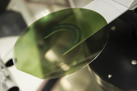
STMicroelectronics unveils 200 mm silicon carbide wafers

Semiconductor company STMicroelectronics has manufactured its first 200 mm (8″) silicon carbide (SiC) bulk wafers for prototyping next-generation power devices at its facility in Norrköping, Sweden. The transition to 200 mm SiC wafers marks an important milestone in the capacity build-up for ST’s customer programs in automotive and industrial sectors, and should consolidate the company’s lead in the disruptive semiconductor technology that allows for smaller, lighter and more efficient power electronics with a lower total cost of ownership.
Silicon carbide is a compound semiconductor material with intrinsic properties providing superior performance and efficiency over silicon in key, high-growth power applications for electro-mobility (e-mobility) and industrial processes, among others. The disruptive technology allows for more efficient power conversion, lighter and more compact designs, and overall system-design cost savings — all key parameters and factors for success in automotive and industrial systems. 200 mm wafers enable a capacity increase, with almost twice the useful area for manufacturing integrated circuits compared to 150 mm wafers, delivering 1.8–1.9 times as many working chips.
Among the first in the world, ST’s initial 200 mm SiC wafers are designed to be high quality, with minimal yield-impacting and crystal-dislocation defects. The low defectivity has been achieved by building on the know-how and expertise in SiC ingot growth technology developed by STMicroelectronics Silicon Carbide AB (formerly Norstel AB, which ST acquired in 2019). In addition to meeting the quality challenge, the transition to 200 mm SiC substrates requires a step forward in manufacturing equipment and the overall support ecosystem performance. ST, in collaboration with technology partners covering the entire supply chain, is developing its own 200 mm SiC manufacturing equipment and processes.
ST currently manufactures its STPOWER SiC products on two 150 mm wafer lines in its fabs in Catania (Italy) and Ang Mo Kio (Singapore) and performs assembly and test at its back-end sites in Shenzhen (China) and Bouskoura (Morocco). This milestone comes as part of the company’s planned move to more advanced, cost-efficient 200 mm SiC volume production. This transition is within the company’s ongoing plan to build a new SiC substrate plant and source over 40% of its SiC substrates internally by 2024.
“The transition to 200 mm SiC wafers will bring substantial advantages to our automotive and industrial customers as they accelerate the transition towards electrification of their systems and products,” said Marco Monti, President Automotive and Discrete Group, STMicroelectronics. “It is important in driving economies of scale as product volumes ramp. Building robust know-how in our internal SiC ecosystem across the full manufacturing chain, from high-quality SiC substrates to large-scale front- and back-end production, boosts our flexibility and allows us to better control the improvement of yield and quality of the wafers.”
Please follow us and share on Twitter and Facebook. You can also subscribe for FREE to our weekly newsletter and bimonthly magazine.
Fully coupled annealing processor for enhanced problem solving
Researchers have designed a scalable, fully-coupled annealing processor with 4096 spins, and...
STMicroelectronics breaks 20 nm barrier for next-gen microcontrollers
STMicroelectronics has launched an advanced process based on 18 nm Fully Depleted Silicon On...
Chip opens door to AI computing at light speed
A team of engineers have developed a silicon-photonics chip that uses light waves, rather than...


