
Single unit displays flexibility of modular system

In an important development for semiconductor manufacturing, researchers from Fraunhofer Institute for Photonic Microsystems IPMS have developed a method that allows different chip components to be fused almost seamlessly into a single unit.
Fraunhofer IPMS said that by precisely embedding small chiplets into specially structured silicon pockets, the researchers had succeeded in combining the advantages of a compact single chip with the flexibility of modular systems for the first time. The finding demonstrates the feasibility of quasi-monolithic integration (QMI) and bridges the gap between traditional chip packaging and cutting-edge semiconductor manufacturing.
The research comes at a time when demand for greater complexity, computing power and system compactness is pushing a rethink of semiconductor manufacturing. Fraunhofer IPMS is aiming for future-proof microelectronics where systems are as powerful as a single chip, yet offer the flexibility of modular building blocks.
The Institute’s research is part of the APECS pilot line (established under the EU Chips Act). Standing for ‘Advanced Packaging and Heterogeneous Integration for Electronic Components and Systems’, APECS is a European pilot line providing industry, SMEs and research organisations with material support for chiplet innovation, system integration and industrial deployment. By connecting development, testing and pilot-scale manufacturing, APECS intends to accelerate the transition from research to application, thus strengthening Europe’s semiconductor ecosystem.
As part of this initiative, Fraunhofer IPMS is pursuing the quasi-monolithic integration (QMI) approach, which aims to integrate various chip components, such as control electronics, sensors and microelectromechanical systems (MEMS), at the wafer level, while retaining the benefits of a compact single chip. Its researchers have already achieved the first critical milestone of the QMI roadmap.
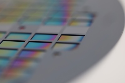
“The basis of QMI is silicon wafers with structured recesses, or pockets. For the first time, dummy chiplets have been inserted into these pocket wafers and the surface has been levelled with a passivation layer in preparation for subsequent back-end-of-line wiring,” said Dr Lukas Lorenz, group leader at Fraunhofer IPMS.
“This creates a nearly monolithic system architecture that combines the highest integration density with modular scalability.”
Technological advantages of QMI
QMI technology offers significant advantages over conventional packaging processes. This is due to the way chiplets are arranged on an active or passive wafer substrate with a shared interconnect stack. Since the interconnects are formed in the front-end-of-line process, much higher connection densities can be achieved than with traditional methods. Benefits include:
- Higher performance: Shorter signal paths reduce losses and latency, thereby increasing processing speed at the system level.
- Reliability: Reducing mechanical interfaces increases the robustness and operational lifetime of the systems.
- Compactness: QMI saves a significant amount of space because the elements are integrated in a nearly monolithic fashion.
- Cost-efficiency: Combining modular chiplet approaches enables highly cost-effective integration, short innovation cycles, and high scalability.
These advantages make QMI suitable for use in highly integrated system-on-chip (SoC) solutions for artificial intelligence (AI) applications and high-bandwidth smart transceivers.
Towards industrial deployment
Lorenz said that although the current demonstrator was based on dummy structures, the process chain can be transferred to real-world customer applications. “This enables a scalable integration architecture for future heterogeneous system solutions,” he said.
With the APECS framework geared towards quickly transferring QMI to production-oriented manufacturing environments, Fraunhofer IPMS is targeting industrial partners whose products could benefit from the integration of different high-density technologies.
New computational method predicts semiconductor properties
A study led by EPFL researchers has introduced a new computational method that predicts the...
3D-printed copper plate could transform data centre cooling
If used to cool an entire data centre, the technology would contribute only about 1.1% of the...
Chiral semiconductors that can absorb visible light
A new system can both absorb visible light and distinguish between left- and right-handed light...


")