Sapphire strain could reshape neuromorphic electronics
Microelectronic devices often depend on super-thin films – sometimes less than 10 nanometres thick — that can switch from blocking to transmitting electricity in response to a small voltage. To work properly in a device, however, these films must be grown on a solid supporting base.
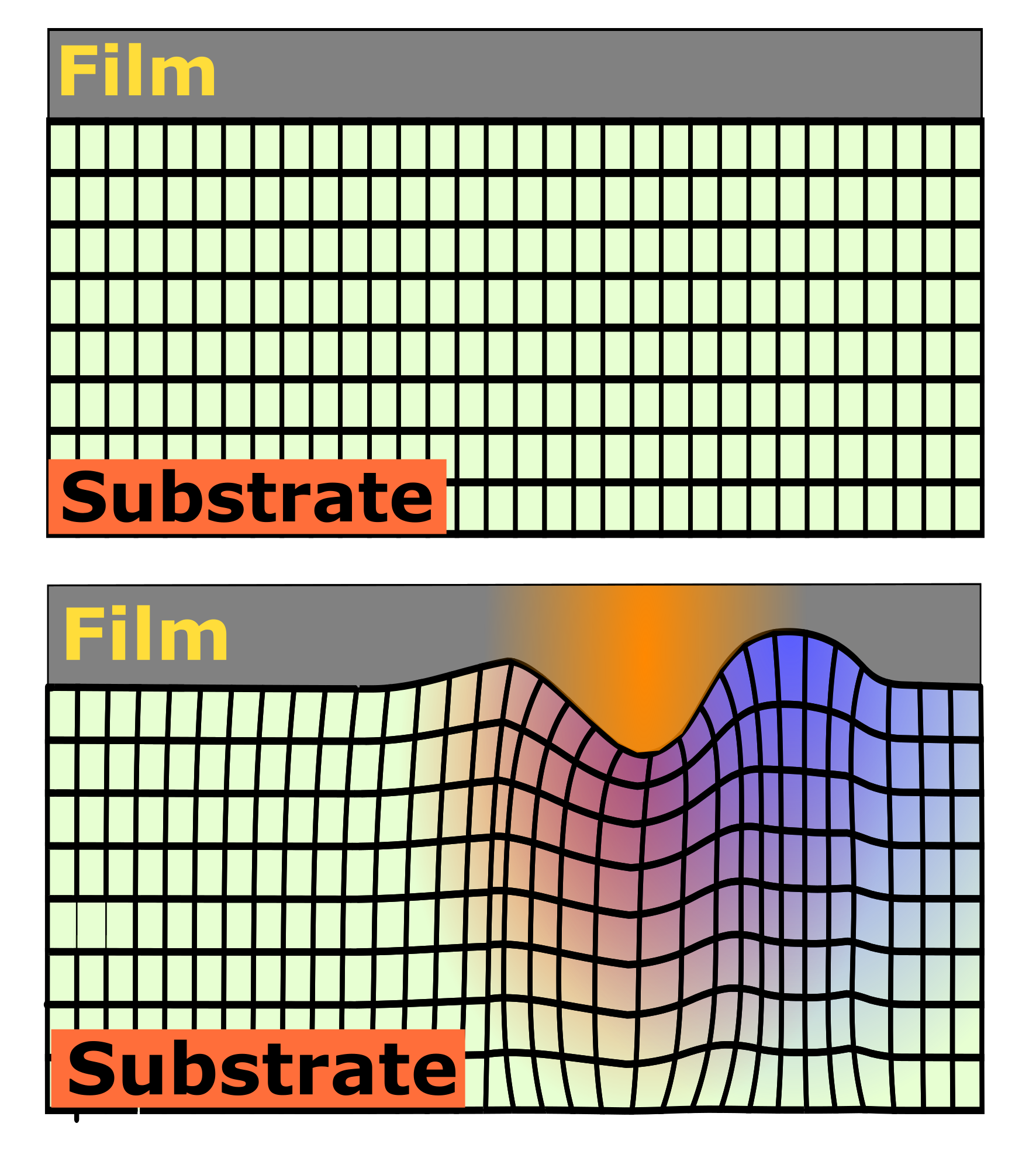
A study by researchers at the U.S. Department of Energy’s (DOE) Argonne National Laboratory and collaborating institutions shows that, in these systems, the base layer is not merely a passive foundation on which a device is fabricated. Working with vanadium dioxide films grown on sapphire, the team found that when the film transitions from electrically insulating to conducting, it strains the sapphire beneath it. The sapphire strain, in turn, feeds back on the film, modifying its behaviour.
The finding challenges a common assumption in microelectronics: that the surface on which the film is grown, called a substrate, simply provides a stable platform for thin-film fabrication, without participating in device operation.
“This is a potentially paradigm-shifting observation,” said Argonne physicist Zahir Islam, a co-author of the study. “You cannot simply assume that the substrate has nothing to do with a device’s properties or behaviour. When the device operates, it can influence the substrate, and that influence surprisingly can propagate much deeper into the substrate than one would expect.”
The team studied vanadium dioxide, a promising material for brain-inspired computing (a ‘memristor’) that has been studied for decades. It behaves in some ways like a neuron in the brain. A neuron may ignore a weak signal the first time it arrives and perhaps the second time as well but it “remembers” those earlier inputs. As signals continue to arrive, even if they are weaker, the neuron eventually responds. Similarly, the memristor remembers previous electrical pulses. By combining memory and action in the same device, memristors can mimic certain features of neural processing while using very little energy.
In the device examined in the study, applying a voltage triggered a localised transition from insulator to conductor, creating a narrow conducting filament within an otherwise insulating film. Because the device retains a memory of prior activation, later switching can occur at lower voltages — a characteristic that makes this memristor attractive for brain-inspired (‘neuromorphic’) computing.
To examine what happens during this transition, the researchers turned to the Advanced Photon Source (APS), a DOE Office of Science user facility at Argonne. At beamlines 6-ID-C and 33-ID-D, they used dark-field X-ray microscopy, an advanced imaging technique, to visualise structural changes across an entire device, including deep beneath the surface.
“When we first saw the unexpected response in the sapphire substrate, we thought it might be an artifact,” said Elliot Kisiel, a Maria Goeppert Mayer fellow at Argonne and a lead author. “Because the result was so surprising, we tested it over and over across multiple devices, samples, film thicknesses and even different substrates. The effect held up.”
At the APS beamlines, the team observed that the filament width expanded with increased voltage and generated an uneven strain in the sapphire beneath it. The distortion extended tens of micrometres into the sapphire — thousands of times deeper than the film thickness itself — and was much larger than would be expected from simple heating alone.
“That depth was a real surprise,” Kisiel said. “A very localised event in a nanoscale film can drive structural changes deep into a rigid substrate. It shows that the mechanical coupling between device and substrate can be long-range.”
The work also highlights the capabilities of the recently upgraded APS. While some of the earliest observations were made before the facility shut down for the upgrade, the improved beam brightness and higher intensity delivered at the sample allowed the team to study many more devices with greater efficiency and sensitivity.
“The brilliance of the APS really shined to bring this work to the finish line,” Islam said. “We were able to study many more devices in far shorter beam time and capture rich structural information with high fidelity.”
Dark-field X-ray microscopy was central to that effort. Unlike techniques that probe only the surface or require destructive sample preparation, it can simultaneously examine interfaces between film and substrate and the bulk substrate underneath.
The findings may have implications beyond thin-film vanadium dioxide. As electronic devices continue to shrink and become more densely packed, substrate-mediated interactions could become either a challenge to overcome or a new feature to exploit. Activity in one device, for example, may mechanically influence neighbouring devices through a shared substrate. This effect may then be engineered to either enhance or hinder such a coupling effect.
That possibility could be particularly relevant for neuromorphic computing. Today’s thin-film devices are only atoms thick, but the brain operates as a densely interconnected 3D network. Understanding and controlling film-substrate interactions could eventually provide new ways to create more complex computing architectures.
Wallpaper generates electricity from moisture in the air
Printable moist-electric generators embedded in wallpaper could harvest indoor humidity to...
New benchmarks for quantum error correction
Researchers from the University of Sydney have found ways to reduce quantum measurement errors,...
Building upward: silicon stacking to extend Moore's law
A new technique for sequentially stacking silicon electronics could increase chip density,...