New form of magnetism could reshape future chips
To build the ultrafast computers of the future, scientists are looking beyond the electrical charge of electrons to another property: their spin. While conventional hardware relies entirely on the movement of charge to process data, the ability to tap into this intrinsic quantum property could enable researchers to completely reinvent how information travels through a circuit.
Now, a team led by UCF Professor of Physics Madhab Neupane has identified a promising candidate. Neupane and his collaborators found evidence of altermagnetism, an emerging form of magnetism that combines useful characteristics of the two more familiar types of magnetism: ferromagnetism and antiferromagnetism.
Ferromagnetism produces the behaviour most people associate with everyday magnets. In these materials, magnetic moments align in the same direction, creating a magnetic field. That property can be useful in electronics, but the resulting stray magnetic fields can interfere with nearby components.
Antiferromagnets behave differently. Their magnetic moments point in opposing directions and cancel one another out, largely avoiding the stray fields. However, they lack some of the useful electronic properties found in ferromagnets.
Altermagnets offer another possibility by combining desirable characteristics of both.
Like antiferromagnets, they can avoid producing unwanted stray magnetic fields. But they can also generate and detect spin currents — the movement of electron spins through a material — that researchers hope to use for future electronics.
Neupane and his collaborators experimentally identified signatures of this unusual magnetic state in Co1/4TaSe2, a layered material containing magnetic cobalt atoms. The discovery gives researchers a promising, versatile platform for studying altermagnetism and could help advance future electronic and spintronic technologies.
“These materials are distinguished from more conventional antiferromagnets by their ability to generate and detect spin currents without the negative effect of producing stray fields,” Neupane said. “This new property makes them very well positioned for use in many different applications — including spintronics, ultrafast memory devices, terahertz networks and energy-efficient electronics.”
Tracking the signs of altermagnetism
To determine whether Co1/4TaSe2 exhibited altermagnetism, the researchers needed to examine how its electrons behaved.
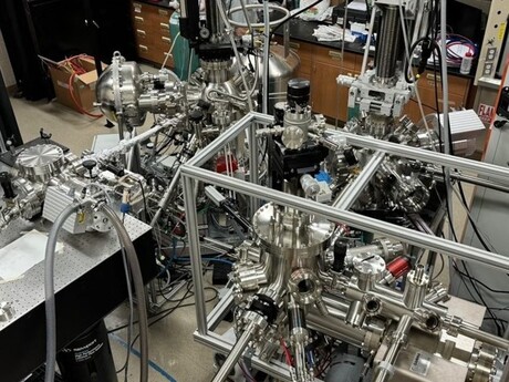
They used a technique called angle-resolved photoemission spectroscopy, or ARPES, which allows scientists to measure the energy and movement of electrons and map a material’s electronic structure.
“Our approach was to use higher-resolution methods that were insensitive to the electron’s spin to measure the splitting in the energy levels,” Neupane said. “Then, we complemented this measurement with spin-resolved ARPES to conclusively tell if this looks like altermagnetism.”
The team first detected a characteristic splitting in the material’s electronic bands. They then used spin-resolved ARPES to take a closer look and found that those split states carried opposite spin polarisations, key evidence of altermagnetism.
Getting a clear look at that behaviour presented another challenge. Photoemission measurements are extremely sensitive to a material’s surface, so researchers needed exceptionally clean samples to accurately observe what was happening.
While collaborators produced high-quality Co1/4TaSe2 samples, Neupane’s team carefully screened them for ultra-clean surfaces before mapping the material’s electronic behaviour.
“The significance became clear once the experimental measurements consistently matched our theoretical predictions,” Neupane said. “Seeing those independent pieces of evidence converge gave us confidence that we had identified a genuine layered altermagnet.”
Why layered materials are changing the game
Finding evidence of altermagnetism was only part of what made Co1/4TaSe2 interesting to researchers.
The material is built from extremely thin layers stacked on top of one another. Because those layers are weakly bound, scientists can separate and combine them into extremely thin structures, making layered materials promising for use in thin-film devices and other emerging technologies.
Scientists call this family of layered materials transition-metal dichalcogenides, or TMDs.
In Co1/4TaSe2, magnetic cobalt atoms inserted between the layers help create the material’s unusual magnetic properties. Its layered structure also makes the material highly tuneable, allowing researchers to modify it and study how those changes affect its electronic and magnetic behaviour.
The team also wanted to understand where that unusual electronic behaviour originated. Before the study, it was unclear whether the key signatures of altermagnetism in layered materials would come primarily from the surface or from deeper within the material.
Their measurements showed that the relevant electronic state originated primarily within the material itself and displayed clear signatures of altermagnetic order.
“Evidence for altermagnetism in a versatile materials platform opens a lot of new possibilities,” said Milo Sprague, the study’s lead graduate student researcher. “There’s currently a lot of debate in altermagnetic theory about how the spin-polarised electronic states interact with other magnetic phenomena. Now we have a material that we can easily modify to explore these new questions.”
Building the foundation for future technologies
Most conventional electronics rely on the electrical charge of electrons to transmit and process information. But electrons possess another property, their spin, that researchers are exploring as another way to carry information.
This emerging field is known as spintronics.
Altermagnets could be particularly useful for spintronics because they can generate and detect spin currents without producing the stray magnetic fields that can interfere with densely packed electronic components.
“As electronic devices continue to shrink, researchers need new materials that can operate faster while consuming less energy,” Neupane said.
Layered materials are already being investigated for use in extremely small transistors, optical technologies and other electronic devices. At the same time, researchers are exploring whether spin currents can provide new ways to transmit digital information.
Layered altermagnets could bring those two areas of research together, providing extremely thin, adaptable materials capable of controlling electron spin without producing the same unwanted magnetic interference as conventional magnets.
“If this approach proves viable, then layered altermagnets will be at the forefront of electronics development,” Neupane said.
What researchers still don’t know
The study gives researchers something particularly valuable: a material they can use to investigate the many unanswered questions surrounding altermagnetism in Co1/4TaSe2.
Scientists still don’t fully understand why this unusual magnetic state forms or why it can become favoured over other possible magnetic structures — including ferromagnetism and other forms of antiferromagnetism — and how it behaves.
Theoretical studies suggest that competition among different interactions between electrons may help determine which magnetic state forms, but researchers are still working to determine how completely those theories describe the behaviour of real materials.
“There are many details to the theory of how altermagnets work that haven’t been explored or verified yet,” Neupane said. “Now that we have identified several platforms for answering these questions, more advanced studies into these materials are underway.”
Because scientists can modify Co1/4TaSe2 and observe how its properties change, the material provides researchers with a new experimental platform for investigating unanswered questions and exploring how altermagnetism interacts with other magnetic and electronic phenomena.
On-chip quantum memory enables longer photon storage times
Researchers have developed a chip-based quantum memory for longer-term photon storage.
Novel semiconductor device enables low-voltage switching
A gallium oxide-based semiconductor device has demonstrated 0.8 V switching, marking a step...
Neuromorphic chip combines sensing, memory and processing
A new neuromorphic vision chip integrates sensing, memory and processing in one system, enabling...