Novel semiconductor device enables low-voltage switching
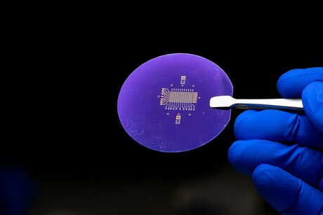
As electronic devices continue to shrink, the materials inside them are being pushed towards an extraordinary limit: the scale of individual atoms.
For future memory and computing technologies, making functional materials thinner could allow more devices to be packed into the same area while reducing the energy required to operate them. But at the atomic scale, simply making a material thinner is not enough. In fact, some of the very properties that make a material useful can begin to disappear.
Ferroelectric materials provide a striking example of this challenge.
Ferroelectrics possess a spontaneous electrical polarisation that can be switched between different states by applying an electric field. Crucially, the polarisation can remain after the external voltage is removed. This ability to ‘remember’ an electrical state makes ferroelectrics attractive for non-volatile memories, in-memory and neuromorphic computing, sensing and other emerging electronic technologies.
However, shrinking a ferroelectric film to only a few atomic layers creates a fundamental dilemma. As the film becomes thinner, depolarisation fields can destabilise its polarisation. At the same time, structural confinement and interface effects can make polarisation increasingly difficult to switch. A material may therefore retain its state very well but require a large voltage to rewrite it — or become easy to switch but unable to reliably retain information.
For advanced electronics, researchers would ideally like to have both: a ferroelectric that is extremely thin and highly stable, yet can still be switched using a low voltage compatible with modern silicon technology.
A research team led by Professor Wei Kong at Westlake University has now demonstrated a new route towards achieving this combination.
In a study published in Nature Electronics, the team reports stable ferroelectric polarisation in single-crystalline 2D-Ga2O3 with a thickness of just 6 angstroms (Å). This corresponds to only half a unit cell of the crystal.
Rather than simply searching for a naturally occurring ultrathin ferroelectric, the researchers took a different approach: they used strain to create ferroelectricity by rearranging the atomic structure of the material.
Making a crystal only half a unit cell thick
Gallium oxide is better known as an ultra-wide-bandgap semiconductor with potential applications in power electronics and optoelectronics. Meanwhile, theoretical studies suggest that ultrathin Ga2O3 could host a rich landscape of novel physical properties, creating new opportunities for fundamental physics research and the development of next-generation ultra-scaled electronic devices.
The first challenge was therefore to prepare high-quality gallium oxide at the extreme thickness required for atomic-scale electronics.
The researchers developed a self-limiting exfoliation strategy based on controlling the epitaxial interface of β-Ga2O3. This enabled them to obtain large-area, single-crystalline films with controllable thicknesses, extending all the way down to half a unit cell.
High-resolution transmission electron microscopy confirmed the crystalline structure of films only 6 Å thick.
But producing an ultrathin crystal was only the beginning. The more important question was whether useful functionality could survive — or even be created — at this scale.
Using strain to give gallium oxide a new property
The key lies in strain.
Atoms in a crystal are arranged in a highly ordered structure. Even when the chemical composition remains unchanged, modifying that arrangement can dramatically alter the physical properties of the material.
The research team found that introducing appropriate strain into ultrathin β-Ga2O3 could drive a structural transformation from its centrosymmetric β phase into a noncentrosymmetric ferroelectric structure.
In simple terms, strain causes the atoms to shift away from their original symmetric positions. Once this symmetry is broken, the material develops a spontaneous electrical polarisation that can point in different directions.
This means that the researchers did not merely preserve an existing ferroelectric property while making the material thinner. Instead, they engineered ferroelectricity through atomic-scale structural control.
A combination of piezoresponse force microscopy and electrical measurements confirmed switchable ferroelectric polarisation in the 6 Å films. The material exhibited a remanent polarisation of approximately 7.5 µC cm-2, together with strong polarisation retention.
The ferroelectric phase also showed remarkable thermal stability, with a Curie temperature above 1300 K.
Stable enough to remember, but still easy to switch
Extreme stability, however, creates another problem.
If the two polarisation states of a ferroelectric are separated by a very high energy barrier, the information can be stored securely, but a large voltage may be needed to switch from one state to the other. This trade-off between retention and switching voltage becomes especially important when ferroelectrics are integrated with advanced complementary metal-oxide-semiconductor (CMOS) electronics, where operating voltages continue to decrease.
The Westlake team found that strain provides a way to tune this balance.
By varying the strain in 2D-Ga2O3, the researchers were able to modify the energy barrier associated with polarisation reversal and reduce the switching voltage to 0.8 V, placing it within a voltage range relevant to advanced CMOS technology.
To understand why such an atomically thin ferroelectric can remain stable while still allowing low-voltage switching, the researchers combined atomic-resolution experiments with density functional theory calculations.
Their results point to an unusual switching mechanism involving covalent-bond reconstruction.
Instead of polarisation reversal occurring solely through a simple displacement of atoms within an otherwise unchanged bonding network, local chemical bonds are reorganised during the switching process. This reconstruction provides a microscopic explanation for the strong stability of the ferroelectric states. At the same time, strain can tune the energy required for this reconstruction, providing a route to lower-voltage operation.
The team further constructed ferroelectric tunnel junction devices based on the material. These devices exhibited an electrical resistance switching ratio of more than 104, demonstrating that the polarisation states can produce a large and measurable electrical response.
From an atomic-scale material to silicon
A promising material for future electronics must ultimately do more than perform well in an isolated laboratory structure. It must also be possible to integrate it with existing semiconductor technologies.
To explore this possibility, the researchers transferred 2D-Ga2O3 films onto different substrates, including SiO2/Si.
Using a low-temperature process compatible with silicon back-end-of-line processing, they were able to activate and retain ferroelectric behaviour after integration on the silicon platform.
This is particularly important because back-end integration offers a potential route to introducing new functional materials after conventional silicon transistors have already been fabricated, without exposing the underlying circuitry to prohibitively high processing temperatures.
The result does not mean that a commercial atomic-scale gallium oxide memory chip is ready to be manufactured. Rather, it shows that the material possesses several characteristics that are difficult to combine in a single ultrathin system: atomic-scale thickness, stable ferroelectricity, low-voltage switching, a large resistance contrast and compatibility with a silicon-oriented integration route.
Engineering function at the atomic scale
The broader significance of the work extends beyond gallium oxide itself.
For decades, miniaturisation has often been framed as a question of whether a material can retain its original properties as its dimensions become smaller. At the atomic scale, however, researchers increasingly have another option: rather than simply preserving existing properties, they can deliberately redesign atomic arrangements, strain states, interfaces and chemical bonding to create new ones.
The 6 Å 2D-Ga2O3 system offers an example of this idea.
Through self-limiting exfoliation, the researchers first created a crystalline material approaching the ultimate thickness limit. Through strain engineering, they then transformed its atomic structure to generate ferroelectricity. Finally, by controlling the switching energy landscape and integrating the film with silicon, they connected the fundamental materials physics with requirements relevant to future electronic devices.
Such an approach could provide new opportunities for high-density non-volatile memories, low-power electronics, computing-in-memory architectures and multifunctional devices that combine computing, storage and sensing.
The study also highlights an emerging principle in nanoscale materials science: when matter becomes only a few atoms thick, size does not have to be merely a limitation. With sufficient control over structure and integration, the atomic scale itself can become a new design space for electronic functionality.
On-chip quantum memory enables longer photon storage times
Researchers have developed a chip-based quantum memory for longer-term photon storage.
Neuromorphic chip combines sensing, memory and processing
A new neuromorphic vision chip integrates sensing, memory and processing in one system, enabling...
Cyborg cockroaches carry electronics into disaster zones
UQ researchers have equipped cockroaches with lightweight electronics, cameras and injectors,...