
300 mm capacity continues to grow, but life remains for 200 mm wafer fabs
Nearly all new fab upgrade and construction activity has to do with 300 mm wafer processing, but there is still plenty of life remaining in 200 mm fabs, according to data in the 2014 edition of IC Insights’ Global Wafer Capacity report.
Not all semiconductor devices are able to take advantage of the cost savings 300 mm wafers can provide. Therefore, fabs running 200 mm wafers will continue to be profitable for many more years to produce several types of ICs such as specialty memories, image sensors, display drivers, microcontrollers and analog products (200 mm fabs are also used for manufacturing MEMS-based ‘non-IC’ products such as accelerometers). These devices can be manufactured in fully depreciated 200 mm fabs that were previously used to make ICs that are now produced on 300 mm wafers.
Wafers measuring ≤150 mm are also forecast to increase slowly throughout the forecast period to meet the growing demand for products such as general-purpose analog chips that can be cost-effectively manufactured on the smaller wafers.
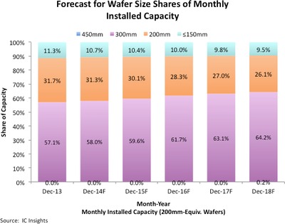
For the most part, 300 mm fabs will continue to be limited to production of high-volume, commodity-type devices like DRAMs and flash memories, complex logic and microcomponent ICs with large die sizes, image sensors and power management devices; and products manufactured by foundries, which can fill a 300 mm fab by combining wafer orders from many sources. IC Insights projects that more than 105 wafer fabs will be producing 300 mm wafer fabs in 2018.
This number includes pilot- and volume-production class fabs, but not research and development facilities. Also, ‘phases’ are counted as separate fabs (eg, TSMC’s Fab 14 currently has four phases for a total of 180K wafers/month).
Additional information and forecasts of the IC industry’s wafer fab capacity through 2018 are provided in IC Insights’ Global Wafer Capacity 2014 - Detailed Analysis and Forecast of the IC Industry’s Wafer Fab Capacity report. Released in December 2013, the Global Wafer Capacity report assesses the IC industry’s capacity by wafer size, minimum process geometry, technology type, geographic region, and by device type through 2018. The report also includes detailed profiles of the companies most likely to build 450 mm wafer fabs and gives detailed specifications on existing wafer fab facilities.
Comau and Omron Robotics to expand industrial automation solutions
The partnership will focus on high-growth sectors including electronics, semiconductors, medical...
Advantech drives innovation at ASEAN Connect 2026
The ASEAN Connect Conference brought together industry leaders to explore Edge AI, foster...
Australia sets path with National Semiconductor Roadmap
The Semiconductor Sector Service Bureau is leading the development of Australia's National...


")