
Diamond film boosts heat dissipation efficiency of GaN HEMTs

Fujitsu and Fujitsu Laboratories have successfully developed what they claim is the world’s first technology for growing a diamond film with highly efficient heat dissipation on the surface of gallium nitride high electron mobility transistors (GaN HEMTs), which are used in power amplifiers for technologies like weather radars and communications equipment.
The design is said to reduce the amount of heat generated by the devices during operations by 40%, leading to simplification of the cooling system and making it possible to miniaturise radar systems that rely on GaN HEMTs. This improvement to the design should make it significantly easier to install larger numbers of the devices for applications including improved weather forecasting and 5G communications.
In recent years, GaN HEMTs have been widely used as transistors for high-frequency amplifiers in weather radar and wireless communications. In the future, achieving breakthroughs in areas like the highly accurate observation of localised torrential downpours and the creation of a stable millimetre-wave high-speed communication environment for 5G communications will make it necessary to increase the number of radars and base stations deployed in the world by a considerable degree.
Limitations inherent to existing designs continue to prevent an increase in the number of installations, however. The transistors used in radar systems have higher output power due to the need to operate at longer distances, which increases the amount of heat they generate. Cooling equipment is required because of the performance degradation caused by overheating. This remains expensive, and the large size of the entire system, including the cooling apparatus, limits the installation location, making simplification and miniaturisation of the cooling equipment an important challenge for designers.
One possible way to reduce the size and complexity of the cooling system is to increase heat dissipation efficiency by covering not only the back surface of the GaN HEMT but also the front surface with a diamond film. This diamond film, which possesses excellent heat dissipation properties, would effectively lower the internal temperature of the GaN HEMT. In order to achieve this effect, however, a diamond crystal with a large grain size is required to pass heat efficiently so that heat does not accumulate inside the diamond. A high temperature of about 900°C is usually required to grow such a diamond film, which unfortunately destroys the GaN HEMT underlying the diamond growth.
When a diamond film is grown at low temperature (~650°C) at which the GaN HEMT is not destroyed, the resulting reduction in thermal energy given to the methane gas used to create the diamond means that the growth of the diamond is incomplete. Using the low-temperature method, it is only possible to grow microscopic diamond particles (or nanodiamonds) of several hundred nanometres or less. Furthermore, each particle becomes an aggregate of crystals facing different directions, which inhibits efficient heat transfer between particles (Figure 1).

The new technology
To address this challenge, Fujitsu has developed a technology for growing a highly heat-spreading diamond film at low temperatures (about 650°C) where transistors are not destroyed, and succeeded in demonstrating the operation of a GaN HEMT with a highly heat-spreading diamond film on its surface.
To grow the diamond film with this method, nanodiamond particles with a diameter of several nanometres are placed on the entire surface of the device. The nanodiamond particles are then exposed to methane gas with high thermal energy to convert the carbon contained in the methane gas into diamond, which can then be incorporated into the particles. Carbon, with its high energy, is selectively incorporated into diamonds that point in a particular direction, allowing diamonds that point in the same direction to bond together and grow.
Focusing on the fact that the thermal energy given to methane varies depending on the pressure and the concentration of methane gas during diamond growth, Fujitsu discovered that nanodiamond particles oriented in a specific direction can be selectively enlarged at low temperatures. This makes it possible to convert a nanodiamond into a micrometre-sized diamond 1000 times larger (Figure 2). As a result, heat can easily pass through the diamond and the GaN HEMT can dissipate heat efficiently.
Outcome
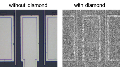
By using the newly developed technology, the amount of heat generated during GaN HEMT operation is reduced by approximately 40% compared to without diamond film, and the temperature can be lowered by 100°C or more. Furthermore, by combining the heat dissipation from the back side of the GaN HEMTs with single-crystal diamond developed by Fujitsu and silicon carbide bonding technology at room temperature, the front and back sides of the GaN HEMTs can be covered with a diamond film, which is expected to reduce heat generation by approximately 77% (Figure 3).
This enables the use of small cooling devices for high-performance radar systems that previously required large cooling devices, thereby saving space and making it easier to install the large number of units demanded for advanced weather forecasting and communications technologies.

Details of the high-heat-dissipation GaN HEMT amplifiers were presented at the 2019 MRS Fall Meeting & Exhibit, held in Boston in early December. Going forward, Fujitsu aims to commercialise the technology in fiscal 2022 for use in weather radar systems and next-generation wireless communication systems.
Please follow us and share on Twitter and Facebook. You can also subscribe for FREE to our weekly newsletter and bimonthly magazine.
New computational method predicts semiconductor properties
A study led by EPFL researchers has introduced a new computational method that predicts the...
Single unit displays flexibility of modular system
Researchers at Fraunhofer Institute for Photonic Microsystems IPMS have developed a method that...
3D-printed copper plate could transform data centre cooling
If used to cool an entire data centre, the technology would contribute only about 1.1% of the...


")