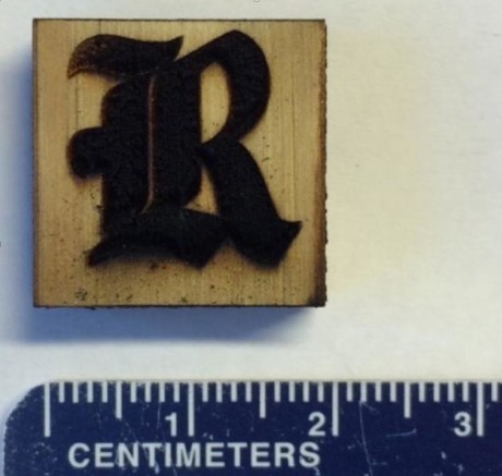
Graphene made from wood

Scientists from Rice University have made wood into an electrical conductor by turning its surface into graphene. Their work has been published in the journal Advanced Materials.
The researchers set out to create what is known as laser-induced graphene (LIG) — a foam of graphene sheets with one edge attached to the underlying surface and chemically active edges exposed to the air. Previous iterations of LIG have been made by heating the surface of a sheet of polyimide, an inexpensive plastic, with a laser.
But not just any polyimide can be used to produce LIG, and the researchers were keen to attempt the synthesis of LIG from non-polyimide materials.
“For some applications, such as three-dimensional graphene printing, polyimide may not be an ideal substrate,” said postgraduate student Ruquan Ye. “In addition, wood is abundant and renewable.”
Led by Ye and fellow postgrad student Yieu Chyan, the research team tried using a laser to blacken a thin film pattern onto birch and oak, but found that pine’s cross-linked lignocellulose structure made it better for the production of high-quality graphene than woods with a lower lignin content. Lignin is the complex organic polymer that forms rigid cell walls in wood.

As with polyimide, the process takes place with a standard industrial laser at room temperature and pressure, and in an inert argon or hydrogen atmosphere. Without oxygen, heat from the laser doesn’t burn the pine but transforms the surface into wrinkled flakes of graphene foam bound to the wood surface.
Changing the laser power also changed the chemical composition and thermal stability of the resulting LIG. At 70% power, the laser produced the highest quality of what the researchers dubbed ‘P-LIG’, where the P stands for pine.
The scientists took their discovery a step further by turning P-LIG into electrodes for splitting water into hydrogen and oxygen and supercapacitors for energy storage. For the former, they deposited layers of cobalt and phosphorus or nickel and iron onto P-LIG to make a pair of electrocatalysts with high surface areas that proved to be durable and effective.
“Because of its high electrical conductivity … graphene patterned on wood surfaces can be readily fabricated into various high-performance devices, such as hydrogen evolution and oxygen evolution electrodes for overall water splitting with high reaction rates at low overpotentials, and supercapacitors for energy storage with high capacitance,” the researchers wrote.

According to Ye, P-LIG could be used in future for the integration of solar energy for photosynthesis. Meanwhile, research leader James Tour sees a more immediate environmental benefit in the form of biodegradable electronics.
“Graphene is a thin sheet of a naturally occurring mineral, graphite, so we would be sending it back to the ground from which it came along with the wood platform instead of to a landfill full of electronics parts,” he said.
Fungi-based semiconductors for flexible electronics
Researchers have harnessed fungi-derived materials to create flexible semiconductors, advancing...
Novel transistor enhances sensing in liquids
Researchers have developed a novel transistor sensor that maintains high accuracy in liquids,...
Photonic AI chip processes data at the speed of light
Aussie researchers have built an ultra-compact nanophotonic AI chip that performs neural network...


