
Light reshapes semiconductors for advanced optical devices

Rice University researchers studying a class of atom-thin semiconductors known as transition metal dichalcogenides (TMDs) have discovered that light can trigger a physical shift in their atomic lattice, creating a tuneable way to adjust the materials’ behaviour and properties.
The effect, observed in a TMD subtype named after the two-faced Roman god of transitions, Janus, could advance technologies that use light instead of electricity, from faster and cooler computer chips to ultrasensitive sensors and flexible optoelectronic devices.
“In nonlinear optics, light can be reshaped to create new colours, faster pulses or optical switches that turn signals on and off,” said Kunyan Zhang, a Rice doctoral alumna who is a first author on a study documenting the effect. “Two-dimensional materials, which are only a few atoms thick, make it possible to build these optical tools on a very small scale.”
TMDs are layered crystals made of a transition metal such as molybdenum and two layers of a chalcogen element like sulfur or selenium. Their combination of electrical conductivity, light absorption and mechanical flexibility has made them one of the most versatile classes of materials for next-generation electronics and optoelectronics.
Within this family, Janus materials stand out for their asymmetry — an idea reflected in their name. Like their mythological namesake, these materials have two different faces: The top and bottom atoms are made of different chemical species, creating an internal imbalance that gives the crystal a built-in electrical polarity, making it sensitive to light and external forces.
“Our work explores how the structure of Janus materials affects their optical behaviour and how light itself can generate a force in the materials,” Zhang said.
Using laser light of different colours, the team studied how a two-layer Janus TMD material — molybdenum sulfur selenide stacked on molybdenum disulfide — converts light through a process called second harmonic generation (SHG), in which the material emits light at twice the frequency of the incoming beam. They found that when the incoming light matched the material’s natural resonances, the doubled-frequency light pattern became distorted, signalling that the atoms inside were being displaced.
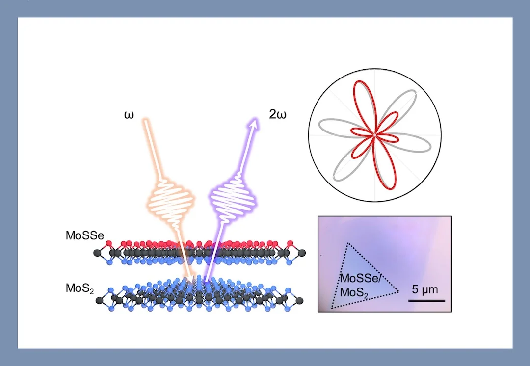
“We discovered that shining light on Janus molybdenum sulfur selenide and molybdenum disulfide creates tiny, directional forces inside the material, which show up as changes in its SHG pattern,” Zhang said. “Normally, the SHG signal forms a six-pointed ‘flower’ shape that mirrors the crystal’s symmetry. But when light pushes on the atoms, this symmetry breaks — the petals of the pattern shrink unevenly.”
The team traced the distortion to optostriction, a process in which the electromagnetic field of light itself exerts a mechanical push on atoms. In Janus materials, that push is amplified by strong coupling between the atomic layers, allowing even minute forces to produce measurable strain.
“Janus materials are ideal for this because their uneven composition creates an enhanced coupling between layers, which makes them more sensitive to light’s tiny forces — forces so small that it is difficult to measure directly, but we can detect them through changes in the SHG signal pattern,” Zhang said.
That sensitivity could make these materials useful far beyond the lab. Components that switch or route light using this principle could make optical chips faster and far more energy-efficient, since light-based circuits generate less heat than conventional electronics. The same responsiveness could be harnessed to create precise sensors capable of detecting the smallest vibrations or pressure changes or tuneable light sources for advanced displays and imaging tools.
“Such active control could help design next-generation photonic chips, ultrasensitive detectors or quantum light sources — technologies that use light to carry and process information instead of relying on electricity,” said Shengxi Huang, an associate professor of electrical and computer engineering and materials science and nanoengineering at Rice, and a corresponding author on the study.
By showing how Janus TMDs’ built-in imbalance opens new ways to steer the flow of light, the study highlights how small structural features can unlock large technological potential.
New computational method predicts semiconductor properties
A study led by EPFL researchers has introduced a new computational method that predicts the...
Single unit displays flexibility of modular system
Researchers at Fraunhofer Institute for Photonic Microsystems IPMS have developed a method that...
3D-printed copper plate could transform data centre cooling
If used to cool an entire data centre, the technology would contribute only about 1.1% of the...
")

