
The future of GaN technology
With benefits such as high switching speeds with low on-resistance and, unlike the bipolar transistors that preceded it, no possibility of thermal runaway, the silicon power MOSFET is the obvious choice in many applications.
Advances in manufacturing technology, allowing the use of a vertical configuration, have delivered devices with many individual transistors in parallel, further lowering their on-resistance.
Over a period of several decades, manufacturers have improved on the basic design, setting new standards in on-resistance and breakdown voltage. However, those parameters generally need to be traded off against each other in MOSFET design. The techniques that increase breakdown voltage tend to push up on-resistance. As a result, inroads have been made by competing devices such as insulated-gate bipolar transistors (IGBTs) for applications that need higher breakdown-voltage ratings than are possible with MOSFETs.
One option is to change materials. Gallium nitride (GaN) and silicon carbide are potential alternatives to silicon that make it possible to support big increases in breakdown voltage without compromising on-resistance thanks to the higher bandgap of these materials, as shown in Figure 1.
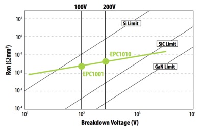
Both SiC and GaN have higher critical electric field strengths than silicon, giving them a superior relationship between on-resistance and breakdown voltage. This allows devices to be made smaller and the electrical terminals brought closer together for a given breakdown-voltage requirement.
GaN is showing promise if not as a replacement for silicon, as a way of extending the reach of the power MOSFET into new and demanding applications. The GaN device is a high electron-mobility transistor (HEMT) that delivers higher electron velocity than is possible with silicon and SiC devices. The high mobility results from the way in which a two-dimensional electron gas forms at the interfaces between the component materials. The carriers in this gas move far more freely than in materials such as silicon. As a result, GaN transistors are far more suitable for high-frequency power switching circuits - potentially delivering higher efficiencies with less board space needed for capacitors and inductors.
Furthermore, GaN devices are able to operate in high-temperature conditions that would be challenging to silicon devices. The high-temperature operation of GaN transistors allows for reductions in the size of heat sinks and cooling fans that may be needed for silicon-based power electronics, allowing for further shrinking of the volume and weight of the power electronics beyond what’s possible from simply moving to higher-frequency switching architectures.
Because of the higher critical field strength, GaN-based devices can be made smaller for a given breakdown voltage and current rating than their silicon counterparts. The combination of device and circuit size, together with less cooling support, leads to overall size and weight savings that are important in transport and defence applications where these are critical parameters.
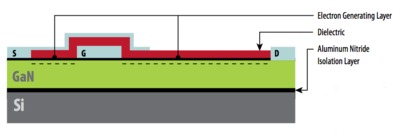
Originally, GaN power devices were constructed on a sapphire substrate and were primarily depletion-mode devices, which made them largely unsuitable for power applications. For safety and reliability reasons, power-switching devices should be designed such that they are normally off. GaN MOSFETs are now appearing that offer enhancement-mode, normally-off operation.
At the same time, silicon is emerging as an effective substrate for GaN, with the advantage of lower cost and compatibility with the existing silicon supply chain. Vendors such as Efficient Power Conversion (EPC) have entered the market with enhancement-mode transistors. Although the number of vendors on the market with commercial GaN-on-silicon transistors is low today, companies such as International Rectifier aim to launch products during 2014.
Even at such an early stage in its development, GaN on silicon is already able to outperform silicon MOSFETs. Figure 1 shows not just the theoretical performance of GaN in terms of breakdown voltage versus on-resistance - both of which easily exceed the capabilities of silicon - but two GaN devices from EPC that are already beyond the silicon line in the graph. Further advantages include low gate leakage current and the material’s large conduction band offset (3.6 eV), making the resulting transistors less susceptible to hot electrons and other factors that can degrade reliability.
As enhancement-mode devices, GaN transistors behave in a similar way to silicon power MOSFETs. A positive gate-source voltage difference attracts electrons into the channel to form a bidirectional channel between the source and drain. As the electrons are pooled in a two-dimension gas, the overall resistance of the conducting channel is very low. However, if the voltage is removed from the gate, the electrons underneath it disperse, removing the conductive channel and turning the device off.
To achieve high breakdown voltages, the distance between drain and gate needs to be increased. However, this does not have as much of an impact on resistance as it does in silicon devices because of the presence of the electron gas.
In contrast to most silicon power MOSFETs, which employ a vertical, through-die channel structure, the GaN transistor structure is lateral, similar to that of logic MOSFET. This structure provides the transistor with a low gate charge, which contributes further to an improved figure of merit (FoM) and very high-performance switching - well into the megahertz range for conventional topologies. This leads to smaller power converters and greater performance in other circuits, such as digital audio amplifiers.
A further benefit of the lateral GaN structure is that there are no minority carriers involved in a conducting device. As a result, there are no reverse recovery losses that tend to limit the switching frequency of silicon devices.
Although the performance of GaN devices is very good, there are considerations that designers need to bear in mind when using them. The ability to switch at high frequency provides new opportunities for power-control topologies, but to achieve high performance with low losses requires careful attention to layout and support-circuit design.
GaN power devices need comparatively low voltages to operate. Full enhancement of the device channel is achieved with a voltage of 5 V between the gate and source. However, it is important to not overdrive the gate - the gate drive level should not exceed the 6 V maximum rating of a typical GaN device to avoid potential damage to its structure. This demands tighter voltage control than is usually the case with silicon devices where loosely regulated transformer-based structures can be used.
Excessive inductance in the gate circuit from devices such as transformers and inductors can easily drive the voltage beyond 5 V for short periods. As the gate inductance increases, voltage ringing becomes stronger, driving up the peak voltage that could damage the gate structure.
A number of techniques can be used to reduce the inductance. One is to use a regulator structure, such as a low-dropout (LDO) device to supply the power for gate drive. PCB techniques can be used to limit the inductance, such as ensuring that the driver is placed close to the device to be driven and that lead lengths are kept shorter than 1 cm. Small-outline packages on drivers intended for high-speed operation will help limit lead inductance. Gate drive and return lines can be placed on top of one another, using stripline techniques, to reduce the loop inductance.
Zener diodes as voltage limiters are not recommended by manufacturers because of their considerable capacitance, which results in slower switching of the GaN transistors, removing one of the key advantages of the GaN material. However, the very fast switching characteristics of GaN introduce a further circuit impact, caused by high dV/dt swings at the drain.
The high levels of dV/dt can cause high current to flow as the result of the Miller capacitance between the gate and drain. In a half-bridge topology a small driver with a relatively high on-resistance can cause the low-side device to turn on accidentally. This phenomenon will increase the risk of shoot-through current and, with that, an increase in wasted energy that will sap the potential efficiency gains that are possible with GaN switches. As a result, the selection of a driver is not only governed by the current and switching time requirement, but also by the need to provide a low impedance path for stray current generated by large dV/dt transients.
Although the GaN on silicon is just beginning to enter the market, current products on the market allow engineers to take advantage of the benefits of the combination of materials using either discrete control or using dedicated support devices.
New computational method predicts semiconductor properties
A study led by EPFL researchers has introduced a new computational method that predicts the...
Single unit displays flexibility of modular system
Researchers at Fraunhofer Institute for Photonic Microsystems IPMS have developed a method that...
3D-printed copper plate could transform data centre cooling
If used to cool an entire data centre, the technology would contribute only about 1.1% of the...


