
The workings of RF transformers - Part 2
Thursday, 03 December, 2009
RF transformers are widely used in electronic circuits for impedance matching to achieve maximum power transfer and to suppress undesired signal reflection. Part 2 of this article continues the story that began in the July issue.
Impedance looking into the secondary winding is measured with the primary winding terminated in its specified impedance (usually 50 or 75 Ω) and compared with the theoretical terminating value (Z2, Z3, or Z4 in Figure 1 [see July’s Part 1]).
Return loss, or VSWR, is measured at the primary winding, with the secondary terminated in its theoretical impedance; eg, 2xZprimary for a 1:2 impedance-ratio (1:1.414 turns-ratio) transformer.
|
|

The performance of RF transformers can be understood with the help of the equivalent circuit in Figure 8.
|
|

L1 and L2 are the primary and secondary leakage inductances, caused by incomplete magnetic coupling between the two windings.
Because their reactance is proportional to frequency, these inductances increase insertion loss and reduce return loss at high frequency.
R1 and R2 are the resistance, or copper loss, of the primary and secondary windings. Skin effect increases the resistance at high frequencies, contributing to the increase in insertion loss.
Intra-winding capacitances C1 and C2, as well as interwinding capacitance C, also contribute to performance limitations at high frequency. However, the distinct advantage of the transmission line design used in RF transformers is that much of the interwinding capacitance is absorbed into the transmission line parameters together with the leakage inductance (parallel capacitance and series inductance), resulting in much wider bandwidth than is obtainable with conventional transformer windings.
Lp is the magnetising inductance, which limits the low frequency performance of the transformer. It is determined by the permeability and cross-sectional area of the magnetic core, and by the number of turns. Insertion loss increases and return loss decreases at low frequency.
Further, permeability of many core materials decreases with a decrease in temperature and increases above room temperature. This accounts for the spread of the lower frequency portion of the insertion loss curves in Figure 3 (see July's Part 1) as earlier explained.
Temperature variation of the capacitances and the leakage inductances is relatively small. The winding resistances do vary, increasing with temperature, and contribute to the spread of the high frequency portion of the curves in Figure 3.
The resistance Rc represents core loss. There are generally three contributions to this loss:
- Eddy-current loss, which increases with frequency;
- Hysteresis loss, which increases with flux density (applied signal level);
- Residual loss, due partially to gyromagnetic resonance.
It is possible to picture the applied RF signal as causing vibratory motion of the magnetic domains of the core material, which behave as particles having inertia and friction. The motion therefore causes a loss of energy. Higher frequency signals cause faster motion, thus greater core loss, and this is represented by a decrease in the value of Rc.
At high temperature, random thermal vibration is greater and adds to the energy which the RF signal must expend to control the movement of the magnetic domains. Thus, core loss contributes to the increase in insertion loss and a decrease in return loss at high frequency. These effects are accentuated at high temperature as shown in Figure 3.
Amplitude balance, sometimes called ‘unbalance’, is the absolute value of the difference in signal amplitude, in dB, between the two outputs of a centre-tapped transformer using the centre tap as a ground reference.
Phase balance, sometimes called ‘unbalance’, is the absolute value of the difference in signal phase between the two outputs of a centre-tapped transformer using the centre tap as a ground reference, after subtracting the 180° nominal value of the phase-split.
It was mentioned earlier that a transformer having a centre-tapped secondary can be tested like a power splitter. There is a difference which must be considered, however.
A device marketed as a power splitter has an internal circuit that provides isolation between the outputs. That provision ensures constant impedance looking into each output port independently of the load on the other output.
A transformer, on the other hand, being a simpler device, lacks isolation. Thus, the design of the matching network must take into account not only the primary source impedance transformed by the primary-to-half-secondary ratio but another impedance in parallel with it: the input impedance of whatever is terminating the other half-secondary winding.
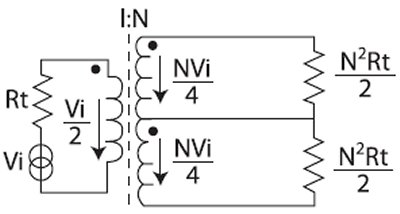
The situation is illustrated in Figure 9. Rt is the source and sensing port impedance of the test instrumentation, as well as the impedance for which the primary of the transformer is designed. The total secondary must be terminated in N2 Rt. Therefore, each matching network, while its output is terminated in Rt, must have an output impedance, ![]() .
.
|
|

The output source impedance of each matching network, because it has to feed a cable presenting a load Rt, must also equal Rt. This must be while the matching network is being fed from a source impedance which is the parallel combination of two impedances as:
One is the transformed source impedance Rt which appears at the half-secondary as (N ÷ 2)2 Rt. The other is the input of the other matching network, N2 Rt ÷ 2, coupled from one half-secondary to the other. The result is N2 Rt ÷ 6.
The impedance constraints for the matching network require three topologies depending on the value of the transformer impedance ratio N2, as shown in Figures 10a to 10c.
|
|

For accurate RF phase balance measurement, the construction of the matching networks and the connections to them should be such as to provide electrical symmetry between the two halves of the circuit.
To show the effectiveness of the above method, it was used to test transformers for amplitude and phase unbalance, with results shown in Figures 11, 12 and 13. These are the same transformers for which insertion loss was given in Figures 5, 6 and 7.
|
|

|
|

|
|

The remaining task is to derive expressions for the insertion loss of the matching network, so that it can be subtracted from measured values to yield insertion loss for the centre-tapped transformer itself when it is tested by the ‘power splitter’ method described above. As a reminder, 3 dB (for the split) must also be subtracted from the measured values.
Figure 14 shows voltage relationships for a transformer with the secondary terminated in matched resistive impedances.
|
|
The voltage across the primary is half the open-circuit source voltage Vi, because the impedance looking into the primary is Rt. The power delivered to each terminating resistor is the square of the voltage divided by the resistance:
![]()
Figure 15 shows what happens when the various matching networks are inserted after the half-secondary and the matched load per Figure 10 is replaced by Rt which represents the sensor port in the instrumentation. Figure 15a includes the ‘N2 <3’ matching network of Figure 10a.
|
|

Table 1 (in July's Part 1) lists the matching-network resistance values, normalised to Rt, as well as the network loss in dB, for values of impedance ratio for which Mini-Circuits offers centre-tapped RF transformers.
Resistors available for the matching networks are typically the ‘1% values’. Their nominal values, having increments of 2%, could thus differ from the Table 1 values of Rs and Rp by as much as ±1%. The resulting error in the loss of the network is greatest if Rs and Rp depart from Table 1 in the opposite direction and amounts to 0.1 dB for N2 = 5, for example, in the case of 1% resistance error.
The information about resistor precision pertains to measurement of insertion loss of a transformer. Amplitude balance is not affected by resistance error as long as the two matching networks are equal.
New computational method predicts semiconductor properties
A study led by EPFL researchers has introduced a new computational method that predicts the...
Single unit displays flexibility of modular system
Researchers at Fraunhofer Institute for Photonic Microsystems IPMS have developed a method that...
3D-printed copper plate could transform data centre cooling
If used to cool an entire data centre, the technology would contribute only about 1.1% of the...
")

