2D dielectric inks for print-in-place electronics

Researchers from The University of Manchester and Duke University have produced a two-dimensional hexagonal boron nitride ink, which has been used to fabricate flexible thin-film transistors.
The insulating dielectric ink is said to be suitable for the print-in-place fabrication process, developed at Duke University for materials such as silver nanowires and semiconducting carbon nanotubes. Extending this process to include the hexagonal boron nitride ink led to the production of functional transistor devices, using both one- and two-dimensional materials.
The use of printing technologies for flexible electronics has increased in prominence due to its simplicity, low cost and compatibility with a broad range of materials and substrates. Currently, there are a wide variety of printable functional inks, often made from organic-based materials or metal oxides; however, problems such as low carrier mobility, poor air stability and the requirement for high processing temperatures are often encountered, limiting their application, the choice of printing method and the substrate which can be printed on.
Traditionally, there has been a particular lack of printable insulating materials that are functional without the use of high processing temperatures. Previous work carried out at Duke had used silicon-based insulating materials, which are typically non-printable, rigid and brittle, thereby limiting the usage of devices in flexible electronic applications.
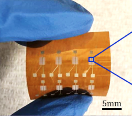
Using the insulating hexagonal boron nitride ink, the team was able to fully fabricate the thin-film transistors with carbon nanotube channel regions via direct-write aerosol jet printing onto flexible paper and plastic substrates in a print-in-place process, with the temperature always below 80°C. This processing temperature is believed to be one of the lowest ever reported for printed carbon nanotube-based thin-film transistors, yet the devices still show good electrical performance. The print-in-place aspect also removes the time and cost associated with the typical processing and treatment steps that are required to be performed outside of the printer.
Published in the journal ACS Nano, the study is amongst the first reports on aerosol printing of 2D materials. Advantages of aerosol jet printing compared to inkjet printing are the ability to print inks with a wide range of viscosity and surface tensions, in addition to the ability to print on complex surfaces.
“We had previously used our hexagonal boron nitride inks to inkjet print a graphene-based transistor on paper,” said Professor Cinzia Casiraghi, who led the team at The University of Manchester. “However, high-performance transistors require a semiconducting channel, so we were pleased to see that our hexagonal boron nitride inks also perform very well in printed carbon nanotubes transistors made with the aerosol printer, showing the versatility of the hexagonal boron nitride inks in printed transistors.”
Dr Aaron Franklin, from Duke University, added, “Nobody thought the aerosolised ink, especially for boron nitride, would deliver the properties needed to make functional electronics without being baked for at least an hour and a half. But not only did we get it to work, we showed that baking it for two hours after printing doesn’t improve its performance. It was as good as it could get just using our fully print-in-place process.”
The team at Duke University hopes to use these inks to devise a fully print-in-place technique for electronics that is gentle enough to work on delicate surfaces, including human skin.
Please follow us and share on Twitter and Facebook. You can also subscribe for FREE to our weekly newsletter and bimonthly magazine.
AI workflow accelerates semiconductor materials discovery
Researchers from the University of New South Wales have developed an AI-driven system to...
Monash reveals atomic switching in new memory tech
Researchers have captured atomic motion behind memory switching, revealing how data is written...
Red OLED microdisplay for energy-efficient AR/VR
Researchers have developed a CMOS-based red OLED microdisplay with luminance and improved power...


