2D semiconductors could have built-in memory functions

Researchers from The University of Manchester’s National Graphene Institute (NGI) and the National Physical Laboratory (NPL) have demonstrated that slightly twisted 2D transition metal dichalcogenides (TMDs) display room-temperature ferroelectricity. This characteristic, combined with TMDs’ outstanding optical properties, can be used to build multifunctional optoelectronic devices such as transistors and LEDs with built-in memory functions on the nanometre scale.
Ferroelectrics are materials with two or more electrically polarisable states that can be reversibly switched with the application of an external electric field. This material property is ideal for applications such as non-volatile memory, microwave devices, sensors and transistors. Until recently, out-of-plane switchable ferroelectricity at room temperature had been achieved only in films thicker than 3 nm.
Since the isolation of graphene in 2004, researchers across academia have studied a variety of new 2D materials with a wide range of exciting properties. These atomically thin 2D crystals can be stacked on top of one another to create so-called heterostructures — artificial materials with tailored functions.
More recently, NGI and NPL researchers demonstrated that below a twist angle of 2°, atomic lattices physically reconstruct to form regions (or domains) of perfectly stacked bilayers separated by boundaries of locally accumulated strain. For two monolayers stacked parallel to each other, a tessellated pattern of mirror-reflected triangular domains is created. Most importantly, the two neighbouring domains have an asymmetric crystal symmetry, causing an asymmetry in their electronic properties.
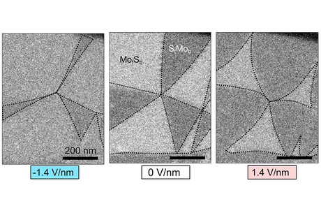
In the work, published in the journal Nature Nanotechnology, the team demonstrated that the domain structure created with low-angle twisting hosts interfacial ferroelectricity in bilayer TMDs. Kelvin probe force microscopy revealed that neighbouring domains are oppositely polarised and electrical transport measurements demonstrated reliable ferroelectric switching at room temperature.
The team went on to develop a scanning electron microscope (SEM) technique with enhanced contrast, using signal from back-scattered electrons. This made it possible to apply an electric field in situ while imaging changes to the domain structure in a non-invasive manner, providing essential information on how the domain switching mechanism works. The boundaries separating the oppositely polarised domains were found to expand and contract depending on the sign of the applied electric field and led to a significant redistribution of the polarised states.
This work clearly demonstrates that the twist degree of freedom can allow the creation of atomically thin optoelectronics with tailored and multifunctional properties.
“It’s very exciting that we can demonstrate that this simple tool of twisting can engineer new properties in 2D crystals,” said lead author Astrid Weston, from the NGI. “With the wide variety of 2D crystals to choose from, it provides us with almost unlimited scope to create perfectly tailored artificial materials.”
“Being able to observe the pattern and behaviour of ferroelectric domains in structures that have nanometre thickness with KPFM and SEM was very exciting,” added co-author Dr Eli G Castanon, from the NPL. “The advancement of characterisation techniques together with the extensive possibilities for the formation of novel heterostructures of 2D materials paves the way to achieve new capabilities at the nanoscale for many industries.”
Please follow us and share on Twitter and Facebook. You can also subscribe for FREE to our weekly newsletter and bimonthly magazine.
AI workflow accelerates semiconductor materials discovery
Researchers from the University of New South Wales have developed an AI-driven system to...
Monash reveals atomic switching in new memory tech
Researchers have captured atomic motion behind memory switching, revealing how data is written...
Red OLED microdisplay for energy-efficient AR/VR
Researchers have developed a CMOS-based red OLED microdisplay with luminance and improved power...


