Better optoelectronics for smarter smartphones

Smarter smartphones could be on the way, thanks to a new theoretical framework that will help physicists and device engineers to design better optoelectronics. The research, conducted by Queen’s University Belfast and ETH Zurich, could lead to optoelectronic devices with less heat generation and power consumption.
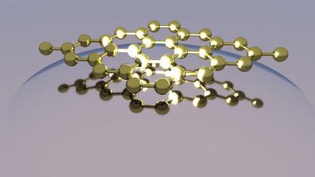
The research enables scientists and engineers to quantify how transparent a 2D material is to an electrostatic field.
“In our paper we have developed a theoretical framework that predicts and quantifies the degree of ‘transparency’ up to the limit of one-atom-thick, 2D materials, to an electrostatic field,” said Dr Elton Santos from the Atomistic Simulation Research Centre at Queen’s.
“Imagine we can change the transparency of a material just using an electric bias, eg, get darker or brighter at will. What kind of implications would this have, for instance, in mobile phone technologies? This was the first question we asked ourselves.
“We realised that this would allow the microscopic control over the distribution of charged carriers in a bulk semiconductor (eg, traditional Si microchips) in a nonlinear manner. This will help physicists and device engineers to design better quantum capacitors, an array of subatomic power storage components capable to keep high energy densities, for instance, in batteries, and vertical transistors, leading to next-generation optoelectronics with lower power consumption and dissipation of heat (cold devices), and better performance. In other words, smarter smartphones.”
Explaining how the theory could have important implications for future work in the area, Dr Santos added, “Our current model simply considers an interface formed between a layer of 2D material and a bulk semiconductor. In principle, our approach can be readily extended to a stack of multiple 2D materials, or namely, van der Waals heterostructures recently fabricated. This will allow us to design and predict the behaviour of these cutting-edge devices in prior to actual fabrication, which will significantly facilitate developments for a variety of applications. We will have an in silico search for the right combination of different 2D crystals while reducing the need for expensive lab work and test trials.”
Further information on the Atomistic Simulation Research Centre at Queen’s is available online at www.titus.phy.qub.ac.uk.
AI workflow accelerates semiconductor materials discovery
Researchers from the University of New South Wales have developed an AI-driven system to...
Monash reveals atomic switching in new memory tech
Researchers have captured atomic motion behind memory switching, revealing how data is written...
Red OLED microdisplay for energy-efficient AR/VR
Researchers have developed a CMOS-based red OLED microdisplay with luminance and improved power...


