Nanosized semiconductors grown on a gold butterfly

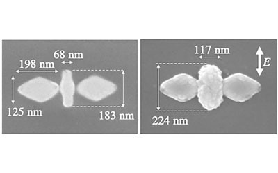
Japanese researchers have devised a way to make nanosized semiconductors on a metal surface, generating localised heat on a gold nanoparticle within a butterfly-shaped nanostructure. The heat causes hydrothermal synthesis in which semiconducting zinc oxide crystallises on the gold nanoparticle.
Scientists have been investigating ways to carefully place nanosized semiconductors on metallic particles to utilise them in nanolasing and nanolithography, for example. But current methods lack precision or are too costly. The researchers from Hokkaido University and Hokkai-Gakuen University developed a new method to overcome these issues, as described in the journal Nano Letters.
The team first conducted simulations to determine the optimal conditions for precisely controlling the generation of heat in nanostructures. They utilised a phenomenon called surface plasmon resonance, a process which partly converts light to heat in metallic materials.
According to the simulations, a butterfly-shaped nanostructure consisting of two rhombus gold particles placed on either side of a gold nanorod would lead to optimal conditions. In this system, the nanorod, or the body of the butterfly, works as a nanoheater using a specific polarised light. After rotating the light polarisation 90°, the rhombus particles, or the wings of the butterfly, should work as an antenna to gather light at subwavelength spots in the butterfly’s semiconductor skin.
To test this theory, the team fabricated the gold butterfly and placed it in water inside a glass chamber. A solution made from equal parts zinc nitrate hexahydrate and hexamethylene tetramine was added to the chamber, which was then sealed and placed on a microscopic stage.
When the laser light was shone on the system inside the chamber, the nanorod heated up and semiconducting zinc oxide particles crystallised along its surface as they expected. This demonstrated that the butterfly-shaped gold nano-antenna can precisely control where plasmon-assisted hydrothermal synthesis occurs, therefore enabling the localised formation of nanosized semiconductors.
“Further research is expected to lead to the development of powerful nanosized light sources, highly efficient photoelectric conversion devices and photocatalysts,” said Hokkaido University’s Keiji Sasaki. “It could also lead to applications in semiconductor electronics and optical quantum information processing.”
Please follow us and share on Twitter and Facebook. You can also subscribe for FREE to our weekly newsletter and bimonthly magazine.
AI workflow accelerates semiconductor materials discovery
Researchers from the University of New South Wales have developed an AI-driven system to...
Monash reveals atomic switching in new memory tech
Researchers have captured atomic motion behind memory switching, revealing how data is written...
Red OLED microdisplay for energy-efficient AR/VR
Researchers have developed a CMOS-based red OLED microdisplay with luminance and improved power...


