Ultra-thin transistors pave way for more efficient chips
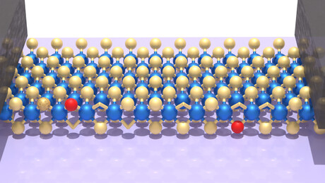
Atomically thin semiconductors can be scaled down to dimensions relevant for future microchips without losing performance, according to a new study published in Nature Nanotechnology. The finding removes a key obstacle to the use of two-dimensional semiconductors in next-generation electronics and could pave the way for more powerful and energy-efficient computing technologies.
Modern computer chips contain billions of silicon transistors — tiny electrical switches that process, store and move information. For decades, shrinking these transistors has been the main way to make electronics faster, more powerful and more energy-efficient. But continuing this trend is becoming harder, as the most critical dimensions in advanced transistors are already measured in just a few nanometres. At these dimensions, silicon, the material that dominates modern electronics, begins to face fundamental material limits.
Among the most promising alternatives are atomically thin materials known as two-dimensional or 2D semiconductors. These materials consist of a thin layer of atoms, which enables low-power electronics thanks to their excellent electrical control. Yet a major question has remained unanswered: can they still perform well at the miniscule dimensions required by future chip technologies?
Now, researchers have fabricated transistors from two-dimensional semiconductors with channel widths as small as 25 nanometres — around 3000 times narrower than a human hair. Despite their tiny size, the devices performed as well as much wider 2D semiconductor transistors. The nanofabrication and electrical characterisation were carried out at Stanford University in the USA, while subsequent analysis was completed at Chalmers University of Technology in Sweden.
“What is particularly encouraging, and actually surprised us, is that the transistors remained well-behaved even when shrunk to dimensions relevant for future industrial technologies. That has been a major uncertainty in the field,” said Anton Persson, assistant professor at Chalmers University of Technology, Sweden, who co-led the study.
While the exceptional thinness of 2D semiconductors has made them attractive for future electronics, researchers have struggled to reduce their width without degrading their performance. As transistors become narrower, their edges play a larger role, raising concerns that defects and damage could limit their performance. The new study shows that this limitation may be less severe than previously feared.
The researchers fabricated nanoribbon transistors using three different atomically thin 2D semiconductors. Across all three materials, the narrow transistors maintained a well-behaved switching behaviour and performance comparable to larger devices.
“The 2D transistors made of tungsten disulfide were especially notable, as their current density improved by more than a hundred times compared to previous demonstrations, thanks to better material quality and improved metal contacts,” Persson said.
The breakthrough was enabled by a combination of innovative device design and advanced nanofabrication techniques. The team developed a so-called ‘dog-bone’ structure, with an extremely narrow transistor channel and wider regions under the electrical contacts to help anchor the material in place.
Towards more sustainable computing
The findings strengthen the case for atomically thin 2D semiconductors as potential building blocks for future generations of electronics.
“Atomically thin 2D semiconductors have many exciting properties that give us a way to explore what may become possible beyond today’s silicon electronics. In the long term, technologies based on these materials could contribute to more powerful and energy-efficient electronics,” Persson said.
Plasma beam antenna transmits radio waves with lasers
A new plasma beam antenna uses laser-generated plasma to transmit radio waves, potentially...
Degrading dopants could enhance semiconductor performance
A new doping method produces up to 100 times more mobile charges in organic semiconductors,...
Nanoscale polar whirlpools emerge in atom-thin semiconductors
Tiny polar whirlpools found in atom-thin tungsten diselenide could enable new approaches to...