Vertical nanowires standing tall

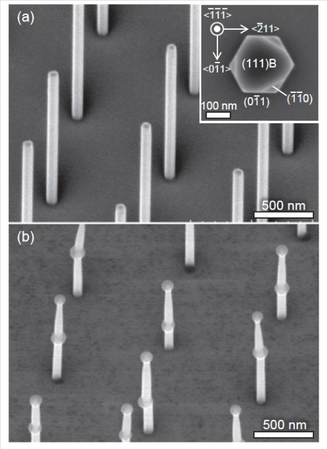
Hokkaido University researchers have demonstrated a method of making vertical nanowires with full control over their size, density and distribution over a semiconducting substrate. Their work contrasts with the current use of bottom-up fabrication techniques that result in vertical nanowires being randomly distributed on semiconducting substrates, limiting their usability.
The team created an indium arsenide (InAs) nanowire template from which to grow the desired heterojunction nanowires, which were composed of ferromagnetic manganese arsenide (MnAs) and semiconducting InAs. They produced the InAs nanowire template by precisely patterning circular openings in silicon dioxide thin films, which were deposited by plasma sputtering onto wafers.
Next, the researchers grew single InAs nanowires in each circular hole. The MnAs nanowires formed either inside (in the middle) or on top of the InAs nanowires by a process known as ‘endotaxy’ — orientated crystal growth inside another crystal. The nanowires had a hexagonal structure, exhibiting no defects or dislocations and no contamination with other elements.
The researchers say their nanowires could prove invaluable in next-generation sensing devices for electronic, photonic and biochemical applications. In fact, the team has already characterised the magnetotransport properties of the nanowires for the potential fabrication of vertical spintronic devices.
The research has been published in the Japanese Journal of Applied Physics.
AI workflow accelerates semiconductor materials discovery
Researchers from the University of New South Wales have developed an AI-driven system to...
Monash reveals atomic switching in new memory tech
Researchers have captured atomic motion behind memory switching, revealing how data is written...
Red OLED microdisplay for energy-efficient AR/VR
Researchers have developed a CMOS-based red OLED microdisplay with luminance and improved power...


