
Efficient switching in IGBT applications
By Matthew Dauterive, Field Application Engineer; Recom Engineering
Monday, 02 December, 2013
As renewable energy takes centre stage, efficiently harvesting this energy becomes increasingly critical. Modular DC/DC converters with dual asymmetric outputs provide the positive and negative voltages as well as the galvanic isolation necessary for IGBT applications.
One main reason for efficiency increases in recent years has been the significant improvement in IGBT performance. IGBTs rapidly switch high voltages (1000 V or more) with extremely low switching losses, making them logical choices when designing inverters and boost converters in power conversion circuits.
In Figure 1, two typical functions of IGBTs in power conversion circuitry are employed. Since DC voltage from the photovoltaic array is unstable and not maximised, a boost converter employing maximum power point tracking (MPPT) is used to acquire the maximum DC voltage from the photovoltaic array further improving performance.

However, this voltage is often useless in DC form. To make it compatible for transmission, it is converted into an AC waveform by using two pairs of bridge-connected antiphase IGBTs. These IGBTs are switched with a PWM signal creating the signal in Figure 1. After passing over an LC filter, it is smoothed and becomes an AC sine wave which can then be injected into a power distribution network.
IGBTs are not only used in power harvesting but in loads as well. Motors control a majority of the world’s electricity, and variable-frequency-drive motors are often the most economic choice. In a typical application (Figure 2), IGBTs are used to adjust the frequency of the AC signal in a variable-frequency-drive three-phase motor. The six-pulse voltage-source inverter drive consists of a bridge rectifier, DC link and inverter. The six IGBTs in the inverter produce the adjustable frequency pulse input to the three-phase motor.
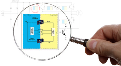
For IGBTs to be an efficient solution, they must be properly driven. Since IGBTs switch at high frequencies up to 300 kHz, typical control circuitry is inadequate. Luckily, drivers were developed in order to allow IGBTs to rapidly switch with minimal losses. Since the driver is connected to the power circuit floating at high voltages, it is isolated from the low-voltage control circuit. An optocoupler isolates the feedback, and the power supply to the driver is galvanically isolated over DC/DC converters. Two separate voltages are used to meet the special conditions when driving an IGBT.
To minimise switching losses, an IGBT switches extremely fast, and the slew rate depends on how fast the gate is charged. Practically, it has been seen that +15 VDC is sufficient to reliably switch on an IGBT, but if the IGBT switches too quickly, the current overshoots, producing a destructive current spike. This not only wreaks havoc with regards to electromagnetic noise, but it also damages the IGBT and its surrounding circuitry. To dampen the spike, it is necessary to increase the switching speed of the IGBT by increasing gate resistance. However, if switching time is increased, then so are the switching losses - and there is part of the dilemma.
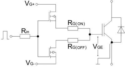
The turn-off behaviour of the IGBT further complicates the matter. Again, the switching rate is determined by the gate capacitance. The faster the gate is discharged, the faster the device turns off. In order to further speed up the discharge of the gate to reduce the switching losses, a negative voltage is applied. Logically, -15 V is considered so one dual-output ±15 V DC/DC converter can be used for both positive and negative rails. However, when the device is switched off too hard, a large destructive voltage spike is created. It is believed that such spikes decrease the life expectancy of IGBTs. Therefore, it becomes necessary to moderate turn-off rates by decreasing the magnitude of the negative voltage on the gate. Practically, -9 VDC is considered to be a nice trade-off. Although switching time is slightly increased leading to larger switching losses, the resultant voltage spikes become manageable.

So there is the full dilemma - either use one ±15 or ±9 VDC dual-output converter and settle for the compromise in either switching losses or destructive voltage spikes, or use two separate DC/DC converters to provide the optimised 15 VDC and -9 VDC which increases component count and design costs. However, there is a third option: use an asymmetrical, dual-output DC/DC converter specially designed for IGBT applications.
The asymmetrical output voltage of these DC/DC converters makes them suitable for supplying the rails which optimise the driving characteristics of IGBTs, but additional information should be considered before selecting the right DC/DC converter. Not only are these converters responsible for supplying the asymmetrical rail voltages, they also provide galvanic isolation which protects the control circuit from high voltages in the power circuit. And without adequate isolation, the entire application fails. But what is adequate isolation?
The level of isolation is often used to describe the isolation of DC/DC converters. Good engineering practice dictates that twice the DC link voltage is a sufficient isolation level. IGBT applications may have a DC link voltage of slightly more than 1000 VDC, so it seems that 2000 VDC should be enough. But it is important to remember the switching spikes at turn-on and turn-off. Furthermore, the parasitic capacitances in the circuit are discharged because of the high slew rate of the IGBT, and the actual voltage levels at switching are much higher. A major hurdle in measurement technology is attempting to measure these spikes in a real application. The inductance of measurement probes actually compromises the measurement, making it nearly impossible to accurately measure these spikes. Since determining the necessary level of isolation is not an exact science, it is a good idea to go as high as reasonably possible. For example, a typical application running with a DC link voltage of 1000 VDC should use an isolation level of 6000 VDC in order to provide continued isolation and extend the lifetime of the system.
While the level of isolation is obviously critical, the type of isolation determined by the construction of the transformer is equally important. Functional isolation relies solely on the transformer wire coating in the DC/DC converter. Once this coating cracks, the isolation of the system fails catastrophically. A better design using basic isolation physically separates input wires from output wires so that even if the wire coating fails, there is still adequate distance between input and output circuits. Since IGBTs often switch at very high frequencies, the isolation is heavily taxed. Therefore, it is recommended that basic isolation is used in order to further extend the lifetime of the system.
When the right DC/DC converter is chosen, IGBT drive circuitry is simplified. Additionally, the life of the application can be extended by making the right choice of switching voltages in order to dampen switching spikes. Moreover, isolation type and level are critical in order to maintain isolation throughout the life of the application. Recom has recently released a family of IGBT converters which meet these demands for IGBT switching applications.
Pressure shown to extend EV battery lifespan
The key to making longer-lasting electric vehicle batteries may not be specialised materials or...
Architecting a better lithium-ion battery
New research has shown that 3D-printed battery electrodes can overcome transport limitations,...
Electrochemical bath revives spent batteries
A novel electrochemical treatment restores battery performance and captures valuable materials,...


")