Perovskite thin film powers devices using indoor light
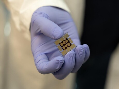
Indoor solar cells, known as photovoltaics, use novel semiconductor materials, such as metal halide perovskite, to convert ambient light into electricity to power small electronic devices without needing batteries or a power outlet.
Now, a team led by materials science researchers at Penn State University has improved perovskite’s ambient light-absorbing ability and its capacity to remain stable over time even at high light intensities.
The research findings have been published in APL Energy.
“The general idea is to try to reduce losses in device performance by finding the right perovskite material and experimenting with what composition performs well and what causes performance losses,” said co-corresponding author Nutifafa Doumon. “Instead of needing to absorb the broad spectrum of light from the sun, indoor photovoltaics only need to absorb the much weaker, narrower spectrum of indoor light.”
To improve the spectrum of light a photovoltaic device can absorb, known as the bandgap, researchers experimented with the material’s ratio of bromine to iodide, two components in perovskite’s crystal structure.
“After understanding how perovskite works and its light absorption profile, I changed the percentage of bromide and iodide incrementally, leading to six different material compositions,” said Justin Lin, lead author of the paper. “I tested the optical properties of all six and gradually shifted the material toward the wavelengths available from indoor lighting to absorb more indoor light. The composition containing 35% bromine was the champion.”
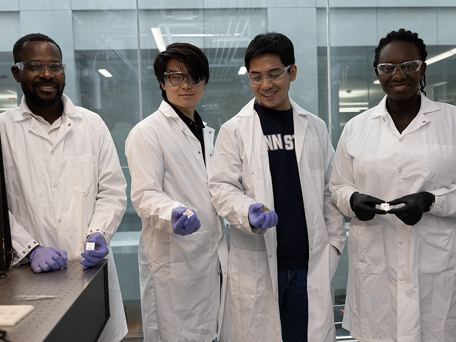
To make a thin film, researchers dissolve materials into a solvent, and as it dries, the perovskite forms a crystal structure. To improve the material’s structure and film quality, researchers used dichlorobenzene as an antisolvent instead of the commonly used chlorobenzene. This decision was based on findings from a 2024 paper by Doumon and Ivy Asuo, assistant professor of materials science and engineering.
“The grains of the thin film should be compact without voids and aligned in a specific direction to improve the quality of the film,” said Asuo, a co-corresponding author of the APL Energy study. “The antisolvent treatments help us drive the crystallisation of perovskite, because you need that for a uniform, high-quality, defect-free thin film, required for photovoltaic performance.”
Finally, researchers added a salt, phenethylammonium bromide, or PEABr, on top of the perovskite layer, forming a passivation layer. The passivation layer adheres to the thin film’s surface to protect it from breaking down under high light intensities over long durations.
“Through testing, we learned that PEABr protected the perovskite layer from defects during the formation of the thin film and reduced loss in perovskite’s ability to absorb ambient light, even at very bright light over long periods of time,” Asuo said.
With the passivation layer, the researchers observed no decline in the device’s performance during 240 hours of testing at high light intensities. Based on that trend, the researchers estimate the device could remain stable for thousands of hours of use.
The device can maintain its performance over time at light intensities approximately 10 to 50 times higher than those required by the new consensus — equivalent to 8 to 50% of the Sun’s brightness.
Looking forward, researchers said they hope to see perovskite-based photovoltaics powering battery-free consumer products, but the technology still has a long way to go.
“Indoor photovoltaics have the potential to power the next generation of consumer devices like smart thermostats, wearable medical devices and TV remotes, but we’re not there yet,” Doumon said. “Because of these materials’ susceptibility to degrading quickly in harsher environments, we need to make them more durable. We also need to improve our ability to accurately measure them.”
Hybrid system integrates power, heating and cooling
A novel hybrid energy system combines electricity generation, heating and cooling under one roof,...
Controlling defects helps improve solar cell performance
UNSW Sydney researchers have uncovered a new way to improve a promising next-generation solar...
Pressure shown to extend EV battery lifespan
The key to making longer-lasting electric vehicle batteries may not be specialised materials or...