Preventing radiation-induced faults in electronics

Electronics exposed to radiation can be prone to failure. Satellites and medical devices such as CT scanners are especially sensitive. Researchers at the Fraunhofer Institute for Integrated Circuits IIS in Dresden are working on an open-source tool that can be used to better prevent radiation-related loss of function.
Telephone and television reception, GPS navigation systems, broadband internet via satellite — none of this would be possible without electronics in space. However, cosmic radiation can damage components, lead to short-term failures, malfunctions and memory errors, and cause the electronics to age more rapidly. Especially affected are satellites, some of which remain in space for several decades, therefore requiring particularly robust and radiation-resistant electronics. The same applies to medical products such as CT scanners, in which high-energy X-rays are used.
To ensure that circuits function reliably in the long term, chip designers must account for stress factors for semiconductor technologies such as radiation bombardment in the design stage. However, smaller companies and research institutions in particular often lack relevant information on the limits and properties of the components implemented in the semiconductor chips. They therefore often have only limited access to innovative technologies.
Researchers at Fraunhofer IIS are working jointly with partners on a solution in the FlowSpace project: “We want to make electronics even more robust and reliable with an open-source tool,” said Roland Jancke, Head of Design Methodology in the Engineering of Adaptive Systems division at Fraunhofer IIS.
According to Jancke, the open-source tool and an open process design kit (PDK) could give a broad community such as universities and smaller companies access to innovative technologies. An open PDK provides an interface between the technologists developing a component and the chip designers. With freely accessible information about the components in the semiconductors, the designers know how these elements behave and can be used.
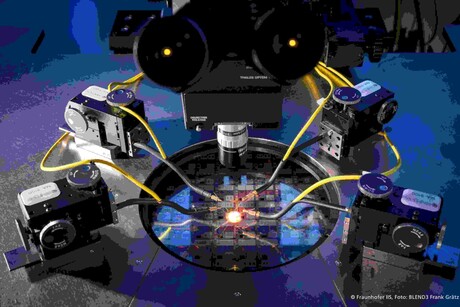
For example, chip designers can already account for component aging in the design phase. In the FlowSpace project, Jancke’s team simulates the long-term response of components to radiation in the laboratory. The scientists use mathematical models and measurements to realistically simulate how a certain component is likely to age, and whether it will still function, after being irradiated over a 10-year period.
Chip developers design relevant circuit parts redundantly for applications exposed to radiation in order to prevent malfunctions. The new solution enables the chip area required for this to be reduced, as it is also compatible with increasingly small semiconductors that are even more sensitive to radiation. Smaller solutions are becoming increasingly popular, as they save energy, space and weight. This is especially important for space modules.
Moiré ferroelectric pixels enable next-gen nanoelectronics
Researchers have demonstrated moiré ferroelectricity in layered nanomaterials, enabling...
Novel technique for tuning superconductivity levels
Researchers have developed a technique to tune superconductivity by adjusting a material's...
Adaptive chip design boosts efficiency in electronics
A new adaptive chip design reduces power use by adjusting performance in real time, boosting...


