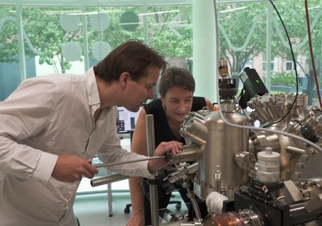
3D atomic-scale quantum chip architecture demonstrated

UNSW scientists at the Centre of Excellence for Quantum Computation and Communication Technology (CQC2T) have shown for the first time that they can build atomic-precision qubits in a 3D device — a major step towards a universal quantum computer. Their work has been published in the journal Nature Nanotechnology.
The researchers, led by CQC2T Director Professor Michelle Simmons, demonstrated that they can extend their atomic qubit fabrication technique to multiple layers of a silicon crystal — achieving a critical component of the 3D chip architecture that they introduced to the world in 2015. According to Prof Simmons, this 3D device architecture is “a significant advancement for atomic qubits in silicon”.
“To be able to constantly correct for errors in quantum calculations — an important milestone in our field — you have to be able to control many qubits in parallel,” Prof Simmons explained.
“The only way to do this is to use a 3D architecture, so in 2015 we developed and patented a vertical criss-cross architecture. However, there were still a series of challenges related to the fabrication of this multilayered device. With this result we have now shown that engineering our approach in 3D is possible in the way we envisioned it a few years ago.”
The team’s solution to these challenges was to build a second control plane or layer of electrodes on top of an initial layer of atomic-scale qubits. They have thus become the first to demonstrate the feasibility of an architecture that uses qubits aligned to control lines — which are essentially very narrow wires — inside a 3D design.
“It’s a highly complicated process, but in very simple terms, we built the first plane and then optimised a technique to grow the second layer without impacting the structures in first layer,” explained Dr Joris Keizer, CQC2T researcher and co-author on the study.
“In the past, critics would say that that’s not possible because the surface of the second layer gets very rough, and you wouldn’t be able to use our precision technique anymore; however, in this paper we have shown that we can do it, contrary to expectations.”
Furthermore, the team members demonstrated that they can align these multiple layers with nanometre precision. Dr Keizer noted, “If you write something on the first silicon layer and then put a silicon layer on top, you still need to identify your location to align components on both layers. We have shown a technique that can achieve alignment within under 5 nm, which is quite extraordinary.”
Lastly, the researchers were able to measure the qubit output of the 3D device within one single measurement (‘single shot’) — with very high fidelity — rather than having to rely on averaging out millions of experiments. “This will further help us scale up faster,” Dr Keizer said.
“The ability to pattern in three dimensions, and precisely align our qubits to accurately measure their spin states, is a world first,” Prof Simmons said. “It’s a major step in the development of a blueprint to build a large-scale quantum computer in silicon.”
Please follow us and share on Twitter and Facebook. You can also subscribe for FREE to our weekly newsletter and bimonthly magazine.
Australia sets path with National Semiconductor Roadmap
The Semiconductor Sector Service Bureau is leading the development of Australia's National...
Electronex 2026 to bring electronics innovation to Sydney
Electronex 2026 will return to Sydney's Rosehill Gardens in June, with over 100 electronics...
$6.9m funding to boost Aussie semiconductor packaging tech
The Australian Government has invested $6.9 million to accelerate semiconductor packaging and...


