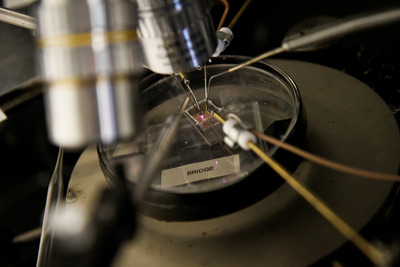
Plasma-based electronics for extreme environs
Small plasma transistors could enable development of smartphones that take and collect medical X-rays on a battlefield and devices to measure air quality in real time.
Massood Tabib-Azar, a professor of electrical and computer engineering at University of Utah, and his doctoral student Pradeep Pai are working on these new transistors.
“These plasma-based electronics can be used to control and guide robots to conduct tasks inside the nuclear reactor,” said Tabib-Azar. “Microplasma transistors in a circuit can also control nuclear reactors if something goes wrong and also could work in the event of nuclear attack.”
Transistors are the workhorses of the electronics industry. They control how electricity flows in devices and act as a switch or gate for electronic signals. Billions of transistors are typically fabricated as individual but connected components on a single computer chip. The most commonly used type of transistor is called a metal oxide semiconductor field effect transistor, or MOSFET.
Transistors control the flow of electrical charge through a silicon channel using an electric field to turn the transistor on or off, similar to a valve with the electric field as its control knob and electric charge as its current flow.
Silicon-based transistors are a crucial component in modern electronics, but they fail above 288°C - the temperature at which nuclear reactors typically operate. Plasma-based transistors, which use charged gases or plasma to conduct electricity at extremely high temperatures, are employed currently in light sources, medical instruments and certain displays under direct sunlight (but not plasma TVs, which are different). These microscale devices are about 500 microns long, or roughly the width of five human hairs. They operate at more than 300 V, requiring special high-voltage sources. Standard electrical outlets in the United States operate at 110 V.

The new devices designed by the University of Utah engineers are the smallest microscale plasma transistors to date. They measure 1 micron to 6 microns in length, or as much as 500 times smaller than current microplasma devices, and operate at one-sixth the voltage. They also can operate at temperatures up to 788°C. Since nuclear radiation ionises gases into plasma, this extreme environment makes it easier for plasma devices to operate.
“Plasmas are great for extreme environments because they are based on gases such as helium, argon and neon that can withstand high temperatures,” says Tabib-Azar. “This transistor has the potential to start a new class of electronic devices that are happy to work in a nuclear environment.”
Traditional MOSFETs require metal to connect circuits, says Tabib-Azar, but the Utah microplasma devices will use a plasma-based connection to enable communication. As a result, these circuits will only be operational when powered up and will disappear otherwise, making them suitable for defence applications.
These plasma devices could also be used as an X-ray imaging source in the next five years, says Tabib-Azar. Because the device dimensions are so small, X-ray images from a wounded soldier in the field could be collected on a smartphone equipped with transistors that also generate the X-rays, says Tabib-Azar.
In another five years, the devices could be used to detect and identify aerosol pollutants based on the colour emitted when the substance passes through the device. “These chemical sensing devices could be used to quantitatively monitor air quality in real time and enable researchers to construct an accurate air-quality map,” he adds.
In the nearer term, these new transistors could be used to generate X-rays to draw fine lines in silicon to pattern microscale devices for the electronics industry. With this new X-ray technique, Tabib-Azar says, “you can do the same thing you would with laser printing, but instead you can use these tiny X-ray sources to print on a silicon wafer. This gives engineers the ability to do X-ray lithography without having to use very heavy lenses and X-ray beam shaping devices.”
Tabib-Azir and Pai’s study has been published in the journal IEEE Electron Device Letters, published by the Institute of Electrical and Electronics Engineers. The study was funded by the Defense Advanced Research Projects Agency.
AI workflow accelerates semiconductor materials discovery
Researchers from the University of New South Wales have developed an AI-driven system to...
Monash reveals atomic switching in new memory tech
Researchers have captured atomic motion behind memory switching, revealing how data is written...
Red OLED microdisplay for energy-efficient AR/VR
Researchers have developed a CMOS-based red OLED microdisplay with luminance and improved power...


