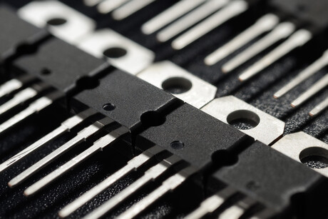
Printing high-performance, perovskite-based transistors

The printing press has long gone beyond simply printing books or documents and is expanding its influence to the realm of cutting-edge technology. Most notably, high-performance components in various smart devices have been successfully printed and have attracted much attention. Now, a new technology to print perovskite-based devices — long considered a challenge — has been proposed.
Researchers led by Professor Yong-Young Noh from the Pohang University of Science and Technology (POSTECH) have improved the performance of a p-type semiconductor transistor using inorganic metal halide perovskite. One of the biggest advantages of the new technology is that it enables solution-processed perovskite transistors to be simply printed as semiconductor-like circuits.
Perovskite-based transistors control the current by combining p-type semiconductors that exhibit hole mobilities (empty spaces created when an electron is subtracted) with n-type semiconductors. Compared to n-type semiconductors that generally have electrons as charge carriers have been actively studied so far, fabricating high-performance p-type semiconductors — which instead have holes as charge carriers — has been a challenge.
Many researchers have tried to utilise perovskite in the p-type semiconductor for its excellent electrical conductivity, but its poor electrical performance and reproducibility have hindered commercialisation. To overcome this issue, the researchers used the modified inorganic metal halide caesium tin triiodide (CsSnI3) to develop the p-type perovskite semiconductor and fabricated the high-performance transistor based on this.
This transistor was found to exhibit high hole mobility of 50 cm2V-1s-1 and higher and a current ratio of more than 108, and recorded the highest performance among the perovskite semiconductor transistors that have been developed so far. The results were published in the journal Nature Electronics.
By making the material into a solution, the researchers succeeded in simply printing the p-type semiconductor transistor as if printing a document. Their method is said to be not only convenient but also cost-effective, which could lead to the commercialisation of perovskite devices in the future.
“The newly developed semiconductor material and transistor can be widely applicable as logic circuits in high-end displays and in wearable electronic devices, and also be used in stacked electronic circuits and optoelectronic devices by stacking them vertically with silicon semiconductors,” Prof Noh said.
Please follow us and share on Twitter and Facebook. You can also subscribe for FREE to our weekly newsletter and bimonthly magazine.
AI workflow accelerates semiconductor materials discovery
Researchers from the University of New South Wales have developed an AI-driven system to...
Monash reveals atomic switching in new memory tech
Researchers have captured atomic motion behind memory switching, revealing how data is written...
Red OLED microdisplay for energy-efficient AR/VR
Researchers have developed a CMOS-based red OLED microdisplay with luminance and improved power...


