
Compact device converts infrared light into images

Electrical engineers at the University of California San Diego (UC San Diego) have developed a novel infrared imager, with potential applications including seeing through smoke and fog, mapping out a person’s blood vessels and inspecting the quality and composition of electronic boards. Their research has been published in the journal Advanced Functional Materials.
The imager detects a part of the infrared spectrum called shortwave infrared light (wavelengths from 1000 to 1400 nm), which is right outside of the visible spectrum (400 to 700 nm). The imager works by shining shortwave infrared light on an object or area of interest, and then converting the low energy infrared light that’s reflected back to the device into shorter, higher-energy wavelengths that the human eye can see.
“It makes invisible light visible,” said Professor Tina Ng, corresponding author on the study.
While infrared imaging technology has been around for decades, most systems are expensive, bulky and complex, often requiring a separate camera and display. They are also typically made using inorganic semiconductors, which are costly, rigid and consist of toxic elements such as arsenic and lead.
The newly developed infrared imager overcomes these issues as it combines the sensors and the display into one thin device, making it compact and simple. It is built using organic semiconductors, so it is low cost, flexible and safe to use in biomedical applications. It also provides better image resolution than some of its inorganic counterparts.
The imager also offers additional advantages. It sees more of the shortwave infrared spectrum — from 1000 to 1400 nm — while existing similar systems often only see below 1200 nm. It also has one of the largest display sizes of infrared imagers to date: 2 cm2 in area. And because the imager is fabricated using thin film processes, it is easy and inexpensive to scale up to make even larger displays.

Energising infrared photons to visible photons
The imager is made up of multiple semiconducting layers, each hundreds of nanometres thin, stacked on top of one another. Three of these layers, each made of a different organic polymer, are the imager’s key players: a photodetector layer, an organic light-emitting diode (OLED) display layer and an electron-blocking layer in between.
The photodetector layer absorbs shortwave infrared light (low-energy photons) and then generates an electric current. This current flows to the OLED display layer, where it gets converted into a visible image (high-energy photons). An intermediate layer, the electron-blocking layer, keeps the OLED display layer from losing any current. This is what enables the device to produce a clearer image.
This process of converting low energy photons to higher energy photos is known as upconversion. What’s special here is that the upconversion process is electronic.
“The advantage of this is it allows direct infrared-to-visible conversion in one thin and compact system,” said first author Ning Li, a postdoctoral researcher in Prof Ng’s lab. “In a typical IR imaging system where upconversion is not electronic, you need a detector array to collect data, a computer to process that data and a separate screen to display that data. This is why most existing systems are bulky and expensive.”
Another special feature is that the imager is efficient at providing both optical and electronic readouts, which makes it multifunctional, Li noted. For example, when the researchers shined infrared light on the back of a subject’s hand, the imager provided a clear picture of the subject’s blood vessels while recording the subject’s heart rate.
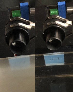
The researchers also used their infrared imager to see through smog and a silicon wafer. In one demonstration, they placed a photomask patterned with ‘EXIT’ in a small chamber filled with smog. In another, they placed a photomask patterned with ‘UCSD’ behind a silicon wafer. Infrared light penetrates through both smog and silicon, making it possible for the imager to see the letters in these demonstrations. This would be useful for applications such as helping autonomous cars see in bad weather and inspecting silicon chips for defects.
The researchers are now working on improving the imager’s efficiency.
Please follow us and share on Twitter and Facebook. You can also subscribe for FREE to our weekly newsletter and bimonthly magazine.
Optimising OEM data for smarter electronics systems
Rockwell Automation's FactoryTalk Optix delivers on-machine monitoring, providing clean,...
Wireless innovation transmits vast amounts of data
Researchers have developed a machine-learning system that curves ultrahigh-frequency signals...
Ricoh chooses u-blox module for long-lasting GNSS performance
The Ricoh Theta X camera incorporates the ZOE-M8B GNSS module from u-blox, allowing users to...
")

