
Faster, simpler 3D printing technique for complex shapes

Engineers from the University of California, Los Angeles (UCLA) have developed a 3D printing technique that they claim to be faster and simpler than current methods, cutting manufacturing time from hours down to a few minutes. Described in the journal Nature Electronics, the method can be used to print electronics into complex shapes in volumes that could be used for antenna arrays, prosthetics, sensors and robots.
Most electronic devices today, including smartphones and laptops, use flat, two-dimensional electronics for components, such as internal sensors or antennas. Three-dimensional electronics can offer curves and shapes that help save space inside devices. Complex shapes, which can only be practically made through 3D printing, can also improve product performance — for example, by making an antenna’s signal stronger.
Current 3D printing methods for electronics use multilayer inks that are electrically conductive. This multistep process can take several hours at a minimum and up to days in order to complete a larger build, and even then it can only yield simple shapes — hence the reason why 3D electronics are not in wide use. To change that paradigm, researchers from the UCLA Samueli School of Engineering developed a two-step method that cuts down the process time to only a few minutes.
First, the team used a single optical 3D printer to pattern 3D shapes with pre-programmed electrostatic charges. Second, the researchers dipped the printed pieces into a solution that contains a dissolved material, such as electrically conducting copper. Within seconds, the material started to organise and stick itself to the designed shapes.
Not only is the new approach much faster, it also allows electronics to be built with complex shapes that have details as small as a few tenths of a millimetre.
“Our much faster and simpler method can open the door to integrating new classes of 3D electronics, such as lighter, more compact antennas for the next generation of smartphones and 5G communications, or new classes of sensors and smart materials for wearables,” said UCLA Assistant Professor Xiaoyu ‘Rayne’ Zheng, principal investigator of the research, who leads a research lab that combines additive manufacturing techniques with smart materials. He added that the new method could also be used in tactile sensors found in ultrasound machines and soft-bodied robots.
The key in instantly programming conducting materials into any predesigned 3D features is harnessing electrostatic attraction — the same phenomenon that explains why a balloon sticks to a wall after rubbing it against one’s hair. As explained by UCLA graduate student Ryan Hensleigh, lead author of the study, “Imagine having a blank grid with squares you can mark black, grey or white — that’s sort of the same idea here as we program where electrodes go. Pixel by pixel, we fill a patterned grid with materials that are positively or negatively charged, or neutral.
“We then use this pattern of electric charge to deposit electrodes, conducting materials and semiconducting materials throughout the surface of a 3D-printed product.”
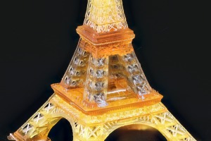
To demonstrate their technique’s capabilities, the researchers printed several devices, including artificial fingertips that can feel the outlines of shapes and points of pressure. The lattice-like sensor has surface and internal electrodes that detect shapes when they’re being squeezed. The team also built a 5 cm-tall detailed model of the Eiffel Tower, with electrodes running throughout its structure, in order to show how the method can be used to produce electronics with complex structure.
Zheng said the new approach can also unite multiple materials in a finished product, which the previous methods failed to accomplish. This may include magnetic materials, semiconducting materials, ceramics, piezoelectrics and carbon nanotubes.
Please follow us and share on Twitter and Facebook. You can also subscribe for FREE to our weekly newsletter and bimonthly magazine.
Wearable glove turns data into thermal sensations
A new wearable glove converts digital information into thermal sensations, allowing users to feel...
Framework enhances synthetic data for AI training
Researchers have developed a set of metrics to evaluate the affinity and diversity of synthetic...
Layered semiconductor shows potential for memory storage
Researchers have discovered that a unique semiconductor undergoes notable structural changes...


