Photonic chip processes images in nanoseconds

Researchers from Tsinghua University have demonstrated an intelligent photonic-sensing computer chip that can process, transmit and reconstruct images of a scene within nanoseconds. This could help facilitate high-speed image processing, to benefit edge intelligence for machine vision applications such as autonomous driving, industrial inspection and robotic vision.
Edge computing, which performs intensive computing tasks like image processing and analysis on local devices, is evolving into edge intelligence by adding artificial intelligence (AI-) driven analysis and decision-making. Research team leader Lu Fang said capturing, processing and analysing images for edge-based tasks like autonomous driving is limited to millisecond-level speeds due to the necessity of optical-to-electronic conversions. “Our new chip can perform all these processes in just nanoseconds by keeping them all in the optical domain. This could be used to significantly enhance, or even replace, the traditional architecture of sensor acquisition followed by AI post-processing,” Fang said.
The new chip, which the researchers call an optical parallel computational array (OPCA) chip, has a processing bandwidth of up to one hundred billion pixels and a response time of six nanoseconds. The researchers also used the chip to create an optical neural network that integrates image perception, computation and reconstruction. Wei Wu, co-first author of the paper, said the chip and optical neural network could boost the efficiency of processing complex scenes in industrial inspection and help advance intelligent robot technology to a higher level of cognitive intelligence.
Machine vision — which uses cameras, image sensors, lighting and computer algorithms to capture, process and analyse images for specific tasks — traditionally involves converting optical information into digital electrical signals using sensors. These signals are then transmitted over optical fibres for long-distance data transmission and downstream tasks. However, the frequent conversion between optical and electrical signals along with limited advancements in electronic processors presents some challenges for improving the speed and processing capacity of machine vision.
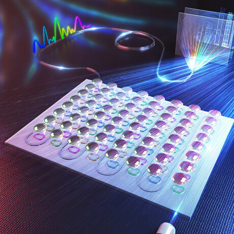
The challenge in performing image acquisition and analysis on the same chip in the optical domain is finding a way to convert the free-space spatial light used for imaging into an on-chip array of dedicated designed ring resonators that convert a free-space optical intensity image into a coherent light signal that can be guided on the chip. A micro-lens array enhances the process by focusing the scene onto the OPCA chip.
The chip’s architecture allowed the researchers to create an end-to-end multi-wavelength optical neural network to couple the on-chip modulated light into a large-bandwidth optical waveguide, where the modulated light is added together spectrally. The multispectral optical outputs can then be used for classification tasks or to create an all-optical reconstruction of the image.
“Because each sensing-computing element of this chip is reconfigurable, they can each operate as a programmable neuron that generates light modulation output based on the input and weight. The neural network connects all the sensing-computing neurons with a single waveguide, facilitating an all-optical full connection between the input information and the output,” Fang said.
Siemens launches AI agent to automate PCB design workflows
Siemens has introduced the Fuse EDA AI Agent to automate workflows across semiconductor, 3D...
Flexible fibre actuator converts electricity into motion
Researchers have developed ultra-thin soft fibres that bend and move when powered by electricity,...
Designing smarter circuits with intelligent tools
Researchers have developed an artificial intelligence technology to automate analog semiconductor...


