3D reflectors help boost data rate in wireless communications

The next generation of wireless communication not only requires greater bandwidth at higher frequencies — it also needs a little extra time.
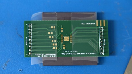
Cornell researchers have developed a semiconductor chip that adds a necessary time delay so signals sent across multiple arrays can align at a single point in space, and without disintegrating. The approach will enable ever-smaller devices to operate at the higher frequencies needed for future 6G communication technology.
The team’s paper, ‘Ultra-Compact Quasi-True-Time-Delay for Boosting Wireless Channel-Capacity’, was published in Nature. The lead author is Bal Govind, a doctoral student in electrical and computer engineering.
The majority of current wireless communications, such as 5G phones, operate at frequencies below 6 gigahertz (GHz). Technology companies have been aiming to develop a new wave of 6G cellular communications that use frequencies above 20 GHz, where there is more available bandwidth, which means more data can flow and at a faster rate. 6G is expected to be 100 times faster than 5G.
However, since data loss through the environment is greater at higher frequencies, one crucial factor is how the data is relayed. Instead of relying on a single transmitter and a single receiver, most 5G and 6G technologies use a more energy-efficient method: a series of phased arrays of transmitters and receivers.
“Every frequency in the communication band goes through different time delays,” Govind said. “The problem we’re addressing is decades old — that of transmitting high-bandwidth data in an economical manner so signals of all frequencies line up at the right place and time.”
This delay has previously been produced by phase-shifting circuits, but they can handle only so much data. That is a particular problem for wideband signals, in which the highest and the lowest frequencies can fall out of phase, causing the signal to blur, a phenomenon known as “beam squint”. And building time delays into a tiny chip that can fit in a smart phone is no small task.
“Most of the way that time delay is constructed is literally by using a long wire that will enable you to delay a signal from point A to point B. And we need that delay to be tuneable so that we can reroute this beam to different locations. We want it to be reconfigurable,” Apsel said.
Govind worked with postdoctoral researcher and co-author Thomas Tapen to design a complementary metal-oxide-semiconductor (CMOS) that could tune a time delay over an ultra-broad bandwidth of 14 GHz, with as high as 1 degree of phase resolution.
“Since the aim of our design was to pack as many of these delay elements as possible,” Govind said, “we imagined what it would be like to wind the path of the signal in three-dimensional waveguides and bounce signals off of them to cause delay, instead of laterally spreading wavelength-long wires across the chip.”
The team engineered a series of these 3D reflectors strung together to form a “tuneable transmission line”.
The resulting integrated circuit occupies a 0.13 mm2 footprint that is smaller than phase shifters yet nearly doubles the channel capacity — ie, data rate — of conventional wireless arrays. And by boosting the projected data rate, the chip could provide faster service, getting more data to cellphone users.
“The big problem with phased arrays is this trade-off between trying to make these things small enough to put on a chip and maintain efficiency,” Apsel said. “The answer that most of the industry has landed on is, ‘Well, we can’t do time delay, so we’re going to do phase delay’. And that fundamentally limits how much information you can transmit and receive. They just sort of take that hit.
“I think one of our major innovations is really the question: Do you need to build it this way?” Apsel said. “If we can boost the channel capacity by a factor of 10 by changing one component that is a pretty interesting game changer for communications.”
Novel transistor enhances sensing in liquids
Researchers have developed a novel transistor sensor that maintains high accuracy in liquids,...
Photonic AI chip processes data at the speed of light
Aussie researchers have built an ultra-compact nanophotonic AI chip that performs neural network...
Detecting ‘mouse bite’ defects in semiconductors
Cornell researchers have used advanced electron microscopy to identify atomic-scale ‘mouse...


