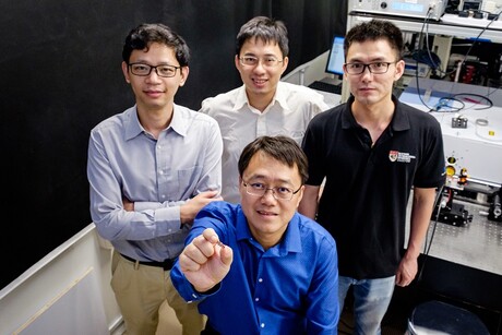
Electrically driven 'topological' laser developed

Scientists and engineers from Nanyang Technological University, Singapore (NTU Singapore) and the University of Leeds have created what they claim to be the first electrically driven ‘topological’ laser, which has the ability to route light particles around corners — and to cope with defects in the manufacture of the device. Their work has been reported in the journal Nature.
Electrically driven semiconductor lasers are the most common type of laser device today. They are used in products such as barcode readers and laser printers, for fibre-optic communications, and in emerging applications such as laser ranging sensors for self-driving cars. However, their manufacture is an exacting process and current laser designs do not work well if any defects are introduced into the structure of the laser during these processes.
The researchers claim to have overcome this longstanding problem, leading to more efficient and less wasteful manufacturing using existing semiconductor technologies. This is accomplished by harnessing a concept from theoretical physics known as the topological states, in order to make a ‘topological laser’.
In the 1980s scientists found that electrons flowing in certain materials have ‘topological features’ — meaning that they can flow around corners or imperfections without scattering or leaking. The Singapore–UK team have now applied this topological approach to light particles, known as photons.
“Every batch of manufactured laser devices has some fraction that fails to emit laser light due to imperfections introduced during fabrication and packaging,” said NTU’s Professor Qi Jie Wang, lead scientist on the project. “This was one of our motivations for exploring topological states of light, which are much more robust than ordinary light waves.”
The researchers worked with a type of electrically driven laser called a quantum cascade laser, based on advanced semiconductor wafers developed at the University of Leeds. To achieve topological states on a laser platform, the team developed a new design containing a valley photonic crystal, which was inspired by electronic topological materials known as two-dimensional valleytronic insulators.
The design consists of hexagonal holes arranged in a triangular lattice, etched into a semiconductor wafer, making it extremely compact. Within the microstructure, the topological states of light circulate within a triangular loop of 1.2 mm circumference, acting as an optical resonator to accumulate the light energy required to form a laser beam.
“The fact that light circulates in this loop, including going around the sharp corners of the triangle, is due to the special features of topological states,” said NTU’s Associate Professor Yi Dong Chong, co-lead investigator on the project. “Ordinary light waves would be disrupted by the sharp corners, preventing them from circulating smoothly.”
The researchers note that an interesting feature of the new topological quantum cascade laser is that the light it emits is at terahertz frequencies between the microwave and infrared regions of the electromagnetic spectrum. Terahertz light has been identified as one of the principal realms from which future technological applications in sensing, illumination and wireless communications may emerge.
“The topological laser is a great example of a fascinating fundamental scientific phenomenon being applied to a practical electronic device and, as our study shows, it has the potential to improve the performance of laser systems,” said Professor Giles Davis, a senior author on the study from the University of Leeds. Looking ahead, the team will be working on lasers that make use of other types of topological states.
“The design we used in this project, called a valley photonic crystal, is not the only way to create topological states,” Prof Wang said. “There are many different types of topological states, imparting protection against different kinds of imperfections. We think it will be possible to tailor the design to the needs of different devices and applications.”
Please follow us and share on Twitter and Facebook. You can also subscribe for FREE to our weekly newsletter and bimonthly magazine.
Chiral semiconductors that can absorb visible light
A new system can both absorb visible light and distinguish between left- and right-handed light...
Pushing the limits of miniaturisation
In a process once thought impossible, a tiny memory chip improves as it gets smaller, potentially...
Fungi-based semiconductors for flexible electronics
Researchers have harnessed fungi-derived materials to create flexible semiconductors, advancing...


