Embedding an antenna into a cellular IoT design

By following some simple design guidelines, a single compact antenna can serve multiple radios in a cellular IoT product.
No matter how much innovation has gone into the design of the hardware and software of a cellular IoT device, if the antenna doesn’t work properly, the product will be useless.
It is the antenna that generates the voltage and current which produces the transmitted electromagnetic (radio) wave, and in turn it’s the antenna across which the incoming radio wave generates the voltage and current picked up by the receiver. Optimising the antenna’s efficiency ensures it converts as much of the transmitter power into radiated radio energy and harvests as much energy as possible from the incoming signal to feed the receiver. This in turn largely determines the range and throughput of the cellular device.
More challenging still, cellular IoT products use radios operating at multiple frequencies. Consider, for example, the Nordic Thingy:91 cellular IoT prototyping platform; the device incorporates an nRF9160 SiP incorporating LTE-M/NB-IoT (operating on several bands in the 700 to 2200 MHz allocation) and GPS (1227 and 1575 MHz), and the nRF52840 SoC (Bluetooth LE operating on 2.4 GHz). It is not uncommon for cellular IoT solutions to also include Wi-Fi (2.4 and 5 GHz). Following conventional design, that means incorporating several different bulky antennas (and their circuitry) into a single product.
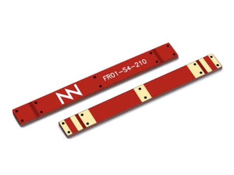
Fortunately, modern chip antenna components offer an elegant solution with compact designs that can cope with the multiple frequencies used by different radios. The single antenna in the Thingy:91, for example, services the platform’s LTE-M/NB-IoT and GPS radios yet measures just 30 x 3 x 1 mm. (A separate antenna serves the Thingy:91’s 2.4 GHz radio.) However, even with these clever chip antennas, there are some sensitivity compromises. That makes it important for the designer to follow some important design guidelines to maximise the antenna’s efficiency and overall frequency response.
Where to place the antenna
The secret to modern chip antenna performance comes from the fact the device itself is only one part of the antenna system. The complete antenna system comprises the chip antenna, PCB ground plane and antenna matching circuit(s). The design of each part of the system directly affects its overall efficiency.
Chip antenna manufacturers, such as Nordic design partner Ignion, have expertise in maximising the antenna’s efficiency for short-range radio and cellular IoT applications. The company also offers an alternative solution for single-, dual- and multiband systems. With knowledge of the end product’s intended operational frequency band(s), it is relatively simple to narrow down the shortlist of suitable chip antennas from the catalogue.
Once the chip antenna has been selected, the next step is to consider the ground plane. The size of the ground plane has a large impact on antenna efficiency. For example, at an operational frequency of 900 MHz, in a like-for-like comparison, a 10 cm2 ground plane might exhibit 30% efficiency where a 40 cm2 ground plane would boost that to 60%. Within the constraints of the end product form factor, it is good design practice to use as large a PCB as possible and then dedicate one complete layer to the ground plane. (As the frequency increases, the ground plane size has less impact on antenna efficiency.)
Next, it’s important to consider where to place the chip antenna on the PCB. A good guideline is to place the antenna at the corner of the device. It is also important to place the chip antenna as far as possible from other active components that could radiate energy during operation. For the transmission power levels typical of cellular IoT devices, a minimum clearance area of 20 mm from other components is satisfactory. The ground plane should be excluded from this clearance area. The only conductors in the clearance area are the PCB pads and traces connecting the chip antenna to the rest of the circuitry. It’s also good practice to keep the antenna away from housing screws, brackets and other metallic parts.

Minimising losses
Perhaps the most important part of the antenna system design is the matching circuit. The matching circuit sits between the chip antenna and the transceiver. Its purpose is to limit the energy reflected from the antenna or due to voltage standing wave ratio (VSWR) when the IoT device is transmitting.
Energy reflection or VSWR is minimised by transforming the antenna impedance to the system impedance (normally 50Ω). The matching network typically comprises inductors and capacitors in a network that transforms the impedance the transceiver ‘sees’ into the antenna in the intended frequency band(s). The use of high-quality factor (Q) and tight tolerance matching network components will enhance performance.
Designing matching networks can be challenging. The trick is to not only to design the appropriate circuit topology but also to select the appropriate inductor and capacitor values to transform the required impedance. For a single operational frequency band (eg, 2.4 GHz), the design is relatively straightforward, but for a cellular IoT product operating in multiple frequency bands the matching circuit becomes much more complex.
The matching network should be placed as close as feasible to the antenna (while maintaining the clearance area) to minimise the length of the connecting traces. Where there must be a trace directly between the transceiver and the antenna, make sure it is designed as a 50Ω transmission line. This minimises trace impedance mismatch and the chance of traces acting as miniature antennas and upsetting the efficiency of the system.
While it is often possible to design a single matching network that works well for a multiband device, this might not always be the case, particularly in a compact device with a small ground plane. An alternative is to design matching networks that work well for each of the intended operational frequency bands and then switch between them as required. Because each network only has to meet the needs of a single frequency band, it can typically be made up of just a few components making it relatively inexpensive and compact. The Nordic Thingy:91, for example, features five matching networks for the various LTE-M/NB-IoT bands and Bluetooth LE, and a further matching network for the GPS signal. (This network also includes an LNA to boost the GPS input to the nRF9160.) Switching between networks is controlled by the nRF9160 SiP’s Arm Cortex M-33 application processor.
Testing the antenna system
The final design must be tested to ensure it not only demonstrates the predicted radiative efficiency but is also approximately omnidirectional (transmits and receives in all directions). The first test can be done by connecting a 50Ω micro-coaxial to the antenna, grounded at three or four points on the PCB and then connecting that cable to a network analyser. The results will not only indicate efficiency but also frequency response and bandwidth. The test typically reveals if some adjustment to the matching network components is needed.
The final examination of the cellular IoT device’s performance should be made in an anechoic chamber. This is the ultimate test of a design and often reveals weaknesses in efficiency and omnidirectional performance that don’t show up during network analyser testing and which require revised chip antenna selection, ground plane and clearance area redesign, and/or matching network tuning.
Even when adhering to proven development techniques, antenna design is challenging and often comes down to repeatedly testing a design’s performance and then refining the layout. Moreover, small antennas are notoriously inefficient. If the design exhibits 50–60% efficiency, the designer has done a decent job. But there are often gains to be made, so it’s always worth a further thorough review of the design.
Please follow us and share on Twitter and Facebook. You can also subscribe for FREE to our weekly newsletter and bimonthly magazine.
Fungi-based semiconductors for flexible electronics
Researchers have harnessed fungi-derived materials to create flexible semiconductors, advancing...
Novel transistor enhances sensing in liquids
Researchers have developed a novel transistor sensor that maintains high accuracy in liquids,...
Photonic AI chip processes data at the speed of light
Aussie researchers have built an ultra-compact nanophotonic AI chip that performs neural network...


